- 您现在的位置:买卖IC网 > PDF目录378277 > ADC08131CIWM (NATIONAL SEMICONDUCTOR CORP) 8-Bit High-Speed Serial I/O A/D Converters with Multiplexer Options, Voltage Reference, and Track/Hold Function PDF资料下载
参数资料
| 型号: | ADC08131CIWM |
| 厂商: | NATIONAL SEMICONDUCTOR CORP |
| 元件分类: | ADC |
| 英文描述: | 8-Bit High-Speed Serial I/O A/D Converters with Multiplexer Options, Voltage Reference, and Track/Hold Function |
| 中文描述: | 1-CH 8-BIT SUCCESSIVE APPROXIMATION ADC, SERIAL ACCESS, PDSO14 |
| 封装: | SOP-14 |
| 文件页数: | 13/21页 |
| 文件大小: | 488K |
| 代理商: | ADC08131CIWM |
Functional Description
(Continued)
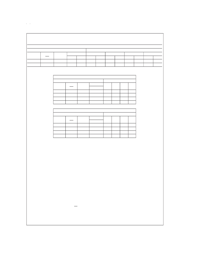
TABLE 3. MUX Addressing: ADC08138
(Continued)
Differential MUX Mode
MUX Address
SGL/
DIF
0
0
Analog Differential Channel-Pair
#
1
2
3
START
ODD/
SIGN
1
1
SELECT
1
1
1
0
2
3
0
0
1
0
1
4
5
+
6
7
1
1
+
TABLE 4. MUX Addressing: ADC08134
Single-Ended MUX Mode
MUX Address
SGL/
DIF
1
1
1
1
Channel
#
1
START
ODD/
SIGN
0
0
1
1
SELECT
1
0
1
0
1
0
2
3
1
1
1
1
+
+
+
+
COM is internally tied to AGND
Differential MUX Mode
MUX Address
SGL/
DIF
0
0
0
0
Channel
#
1
START
ODD/
SIGN
0
0
1
1
SELECT
1
0
1
0
1
0
2
3
1
1
1
1
+
+
+
+
Since the input configuration is under software control, it can
be modified as required before each conversion. A channel
can be treated as a single-ended, ground referenced input
for one conversion; then it can be reconfigured as part of a
differential channel for another conversion. Figure 1 illus-
trates the input flexibility which can be achieved.
The analog input voltages for each channel can range from
50 mV below ground to 50 mV above V
CC
(typically 5V) with-
out degrading conversion accuracy.
THE DIGITAL INTERFACE
A most important characteristic of these converters is their
serial data link with the controlling processor. Using a serial
communication format offers two very significant system im-
provements; it allows many functions to be included in a
small package and it can eliminate the transmission of low
level analog signals by locating the converter right at the
analog sensor; transmitting highly noise immune digital data
back to the host processor.
To understand the operation of these converters it is best to
refer to the Timing Diagrams and Functional Block Diagram
and to follow a complete conversion sequence. For clarity a
separate timing diagram is shown for each device.
1.
A conversion is initiated by pulling the CS (chip select)
line low. This line must be held low for the entire conver-
sion. The converter is now waiting for a start bit and its
MUX assignment word.
2.
On each rising edge of the clock the status of the data in
(DI) line is clocked into the MUX address shift register.
The start bit is the first logic “1” that appears on this line
(all leading zeros are ignored). Following the start bit the
converter expects the next 2 to 4 bits to be the MUX as-
signment word.
When the start bit has been shifted into the start location
of the MUX register, the input channel has been as-
signed and a conversion is about to begin. An interval of
1
2
clock period is automatically inserted to allow for sam-
pling the analog input. The SARS line goes high at the
end of this time to signal that a conversion is now in
progress and the DI line is disabled (it no longer accepts
data).
The data out (DO) line now comes out of TRI-STATE
and provides a leading zero.
During the conversion the output of the SAR comparator
indicates whether the analog input is greater than (high)
or less than (low) a series of successive voltages gener-
ated internally from a ratioed capacitor array (first 5 bits)
and a resistor ladder (last 3 bits). After each comparison
the comparator’s output is shipped to the DO line on the
falling edge of CLK. This data is the result of the conver-
sion being shifted out (with the MSB first) and can be
read by the processor immediately.
After 8 clock periods the conversion is completed. The
SARS line returns low to indicate this
1
2
clock cycle later.
3.
4.
5.
6.
www.national.com
13
相关PDF资料 |
PDF描述 |
|---|---|
| ADC08134CIWM | 8-Bit High-Speed Serial I/O A/D Converters with Multiplexer Options, Voltage Reference, and Track/Hold Function |
| ADC08138CIWM | 8-Bit High-Speed Serial I/O A/D Converters with Multiplexer Options, Voltage Reference, and Track/Hold Function |
| ADC08131 | 8-Bit High-Speed Serial I/O A/D Converters with Multiplexer Options, Voltage Reference, and Track/Hold Function(8位高速串行输入/输出A/D转换器带多路选择,电压基准和跟踪/保持功能) |
| ADC08134 | 8-Bit High-Speed Serial I/O A/D Converters with Multiplexer Options, Voltage Reference, and Track/Hold Function(8位高速串行输入/输出A/D转换器带多路选择,电压基准和跟踪/保持功能) |
| ADC08138 | 8-Bit High-Speed Serial I/O A/D Converters with Multiplexer Options, Voltage Reference, and Track/Hold Function(8位高速串行输入/输出A/D转换器带多路选择,电压基准和跟踪/保持功能) |
相关代理商/技术参数 |
参数描述 |
|---|---|
| ADC08131CIWM/NOPB | 制造商:Texas Instruments 功能描述:ADC Single SAR 8-bit Serial 14-Pin SOIC |
| ADC08131CIWMX | 制造商:未知厂家 制造商全称:未知厂家 功能描述:Analog-to-Digital Converter, 8-Bit |
| ADC08134 | 制造商:NSC 制造商全称:National Semiconductor 功能描述:8-Bit High-Speed Serial I/O A/D Converters with Multiplexer Options, Voltage Reference, and Track/Hold Function |
| ADC08134BIJ | 制造商:未知厂家 制造商全称:未知厂家 功能描述:Single-Ended Data Acquisition System |
| ADC08134BIWM | 制造商:National Semiconductor 功能描述:08134 NAT SEMI |
发布紧急采购,3分钟左右您将得到回复。