- 您现在的位置:买卖IC网 > PDF目录378277 > ADC08138CIWM (NATIONAL SEMICONDUCTOR CORP) 8-Bit High-Speed Serial I/O A/D Converters with Multiplexer Options, Voltage Reference, and Track/Hold Function PDF资料下载
参数资料
| 型号: | ADC08138CIWM |
| 厂商: | NATIONAL SEMICONDUCTOR CORP |
| 元件分类: | ADC |
| 英文描述: | 8-Bit High-Speed Serial I/O A/D Converters with Multiplexer Options, Voltage Reference, and Track/Hold Function |
| 中文描述: | 8-CH 8-BIT SUCCESSIVE APPROXIMATION ADC, SERIAL ACCESS, PDSO20 |
| 封装: | SO-20 |
| 文件页数: | 5/21页 |
| 文件大小: | 488K |
| 代理商: | ADC08138CIWM |
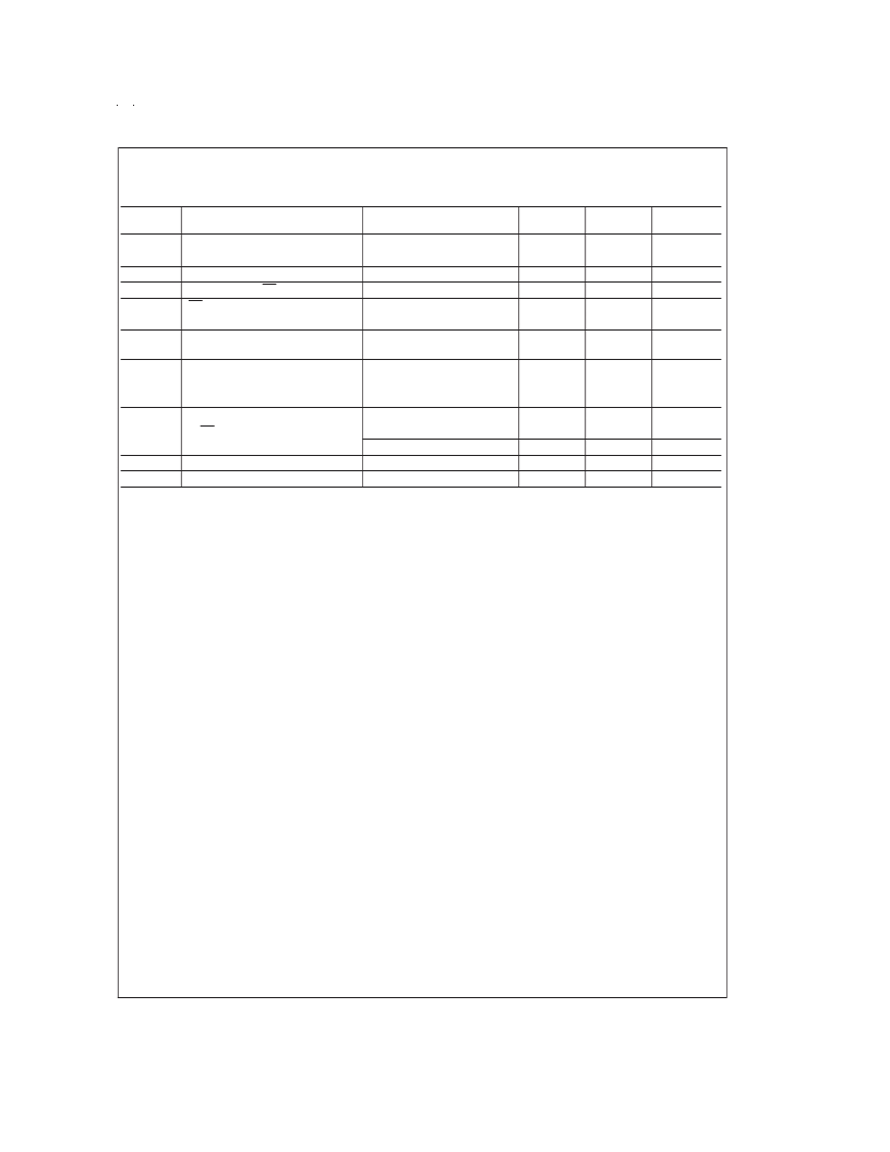
Electrical Characteristics
(Continued)
The following specifications apply for V
CC
= +5 V
, V
= +2.5 V
and t
r
= t
f
= 20 ns unless otherwise specified.
Boldface
limits apply for T
A
= T
J
= T
MIN
to T
MAX
;
all other limits T
A
= T
J
= 25C.
Symbol
Parameter
Conditions
Typical
(Note 8)
Limits
(Note 9)
8
8
Units
(Limits)
1/f
CLK
(max)
μs (max)
1/f
CLK
(max)
ns
T
C
Conversion Time (Not Including
MUX Addressing Time)
Acquisition Time
CLK High while CS is High
CS Falling Edge or Data Input
Valid to CLK Rising Edge
Data Input Valid after CLK Rising
Edge
f
CLK
= 1 MHz
t
CA
t
SELECT
1
2
50
t
SET-UP
25
ns (min)
t
HOLD
20
ns (min)
t
pd1
, t
pd0
CLK Falling Edge to Output Data
Valid (Note 15)
C
L
= 100 pF:
Data MSB First
Data LSB First
C
L
= 10 pF, R
L
= 10 k
(see TRI-STATE Test Circuits)
C
L
= 100 pF, R
L
= 2 k
250
200
ns (max)
ns (max)
t
1H
, t
0H
TRI-STATE Delay from Rising Edge
of CS to Data Output and SARS
Hi-Z
50
ns
180
ns (max)
pF
pF
C
IN
C
OUT
Capacitance of Logic Inputs
Capacitance of Logic Outputs
5
5
Note 1:
Absolute Maximum Ratings indicate limits beyond which damage to the device may occur.
Note 2:
Operating Ratings indicate conditions for which the device is functional. These ratings do not guarantee specific performance limits. For guaranteed speci-
fications and test conditions, see the Electrical Characteristics. The guaranteed specifications apply only for the test conditions listed. Some performance character-
istics may degrade when the device is not operated under the listed test conditions.
Note 3:
All voltages are measured with respect to AGND = DGND = 0 V
DC
, unless otherwise specified.
Note 4:
When the input voltage (V
) at any pin exceeds the power supplies (V
<
(AGND or DGND) or V
>
AV
) the current at that pin should be limited to
5 mA. The 20 mA maximum package input current rating limits the number of pins that can safely exceed the power supplies with an input current of 5 mA to four
pins.
Note 5:
The maximum power dissipation must be derated at elevated temperatures and is dictated by T
,
θ
and the ambient temperature, T
. The maximum
allowable power dissipation at any temperature is P
D
=(T
T
)/
θ
or the number given in theAbsolute Maximum Ratings, whichever is lower. For these devices
T
= 125C. The typical thermal resistances (
θ
JA
) of these parts when board mounted for the ADC 08131 and the ADC08134 is 140C/W and 91C/W for the
ADC08138.
Note 6:
Human body model, 100 pF capacitor discharged through a 1.5 k
resistor.
Note 7:
See AN450 “Surface Mounting Methods and Their Effect on Product Reliability” or Linear Data Book section “Surface Mount” for other methods of soldering
surface mount devices.
Note 8:
Typicals are at T
J
= 25C and represent the most likely parametric norm.
Note 9:
Guaranteed to National’s AOQL (Average Outgoing Quality Level).
Note 10:
Total unadjusted error includes zero, full-scale, linearity, and multiplexer error. Total unadjusted error with V
REF
= +5V only applies to the ADC08134 and
ADC08138. See (Note 16).
Note 11:
Cannot be tested for the ADC08131.
Note 12:
For V
≥
V
the digital code will be 0000 0000. Two on-chip diodes are tied to each analog input (see Block Diagram) which will forward-conduct for
analog input voltages one diode drop below ground or one diode drop greater than V
supply. During testing at low V
levels (e.g., 4.5V), high level analog inputs
(e.g., 5V) can cause an input diode to conduct, especially at elevated temperatures. This will cause errors for analog inputs near full-scale. The specification allows
50 mV forward bias of either diode; this means that as long as the analog V
does not exceed the supply voltage by more than 50 mV, the output code will be correct.
Exceeding this range on an unselected channel will corrupt the reading of a selected channel. Achievement of an absolute 0 V
DC
to 5 V
DC
input voltage range will
therefore require a minimum supply voltage of 4.950 V
DC
over temperature variations, initial tolerance and loading.
Note 13:
Channel leakage current is measured after a single-ended channel is selected and the clock is turned off. For off channel leakage current the following two
cases are considered: one, with the selected channel tied high (5 V
) and the remaining seven off channels tied low (0 V
), total current flow through the off chan-
nels is measured; two, with the selected channel tied low and the off channels tied high, total current flow through the off channels is again measured. The two cases
considered for determining on channel leakage current are the same except total current flow through the selected channel is measured.
Note 14:
A 40% to 60% duty cycle range insures proper operation at all clock frequencies. In the case that an available clock has a duty cycle outside of these limits
the minimum time the clock is high or low must be at least 450 ns. The maximum time the clock can be high or low is 100 μs.
Note 15:
Since data, MSB first, is the output of the comparator used in the successive approximation loop, an additional delay is built in (see Block Diagram) to allow
for comparator response time.
Note 16:
For the ADC08131 V
IN is internally tied to the on chip 2.5V band-gap reference output; therefore, the supply current is larger because it includes the
reference current (700 μA typical, 2 mA maximum).
Note 17:
Load regulation test conditions and specifications for the ADC08131 differ from those of the ADC08134 and ADC08138 because the ADC08131 has the
on-board reference as a permanent load.
www.national.com
5
相关PDF资料 |
PDF描述 |
|---|---|
| ADC08131 | 8-Bit High-Speed Serial I/O A/D Converters with Multiplexer Options, Voltage Reference, and Track/Hold Function(8位高速串行输入/输出A/D转换器带多路选择,电压基准和跟踪/保持功能) |
| ADC08134 | 8-Bit High-Speed Serial I/O A/D Converters with Multiplexer Options, Voltage Reference, and Track/Hold Function(8位高速串行输入/输出A/D转换器带多路选择,电压基准和跟踪/保持功能) |
| ADC08138 | 8-Bit High-Speed Serial I/O A/D Converters with Multiplexer Options, Voltage Reference, and Track/Hold Function(8位高速串行输入/输出A/D转换器带多路选择,电压基准和跟踪/保持功能) |
| ADC081500 | High Performance, Low Power, 8-Bit, 1.5 GSPS A/D Converter |
| ADC081500CIYB | High Performance, Low Power, 8-Bit, 1.5 GSPS A/D Converter |
相关代理商/技术参数 |
参数描述 |
|---|---|
| ADC08138CIWM/NOPB | 制造商:Texas Instruments 功能描述:ADC Single SAR 8-bit Serial 20-Pin SOIC W |
| ADC08138CIWMX | 功能描述:IC ADC 8BIT HS SERIAL I/O 20SOIC RoHS:否 类别:集成电路 (IC) >> 数据采集 - 模数转换器 系列:- 产品培训模块:Lead (SnPb) Finish for COTS Obsolescence Mitigation Program 标准包装:2,500 系列:- 位数:12 采样率(每秒):3M 数据接口:- 转换器数目:- 功率耗散(最大):- 电压电源:- 工作温度:- 安装类型:表面贴装 封装/外壳:SOT-23-6 供应商设备封装:SOT-23-6 包装:带卷 (TR) 输入数目和类型:- |
| ADC08138CIWMX/NOPB | 制造商:Texas Instruments 功能描述:ADC Single SAR 8-bit Serial 20-Pin SOIC W T/R |
| ADC08138CMJ | 制造商:未知厂家 制造商全称:未知厂家 功能描述:Single-Ended Data Acquisition System |
| ADC081500 | 制造商:NSC 制造商全称:National Semiconductor 功能描述:High Performance, Low Power, 8-Bit, 1.5 GSPS A/D Converter |
发布紧急采购,3分钟左右您将得到回复。