- 您现在的位置:买卖IC网 > PDF目录378279 > ADC0833BCN (NATIONAL SEMICONDUCTOR CORP) 8-Bit Serial I/O A/D Converter with 4-Channel Multiplexer PDF资料下载
参数资料
| 型号: | ADC0833BCN |
| 厂商: | NATIONAL SEMICONDUCTOR CORP |
| 元件分类: | ADC |
| 英文描述: | 8-Bit Serial I/O A/D Converter with 4-Channel Multiplexer |
| 中文描述: | 4-CH 8-BIT SUCCESSIVE APPROXIMATION ADC, SERIAL ACCESS, PDIP14 |
| 封装: | 0.300 INCH, PLASTIC, DIP-14 |
| 文件页数: | 12/20页 |
| 文件大小: | 316K |
| 代理商: | ADC0833BCN |
Functional Description
(Continued)
4.0 THE ANALOG INPUTS
The most important feature of these converters is that they
can be located right at the analog signal source and through
just a few wires can communicate with a controlling proces-
sor with a highly noise immune serial bit stream. This in itself
greatly minimizes circuitry to maintain analog signal accura-
cy which otherwise is most susceptible to noise pickup.
However, a few words are in order with regard to the analog
inputs should the inputs be noisy to begin with or possibly
riding on a large common-mode voltage.
The differential input of these converters actually reduces
the effects of common-mode input noise, a signal common
to both selected ‘‘
a
’’ and ‘‘
b
’’ inputs for a conversion (60
Hz is most typical). The time interval between sampling the
‘‘
a
’’ input and then the ‘‘
b
’’ input is
(/2
of a clock period.
The change in the common-mode voltage during this short
time interval can cause conversion errors. For a sinusoidal
common-mode signal this error is:
V
error
(max)
e
V
PEAK
(2
q
f
CM
)
0.5
f
CLK
where f
CM
is the frequency of the common-mode signal,
V
PEAK
is its peak voltage value
and f
CLK
is the A/D clock frequency.
For a 60 Hz common-mode signal to generate a
(/4
LSB
error (
&
5 mV) with the converter running at 250 kHz, its
peak value would have to be 6.63V which would be larger
than allowed as it exceeds the maximum analog input limits.
Due to the sampling nature of the analog inputs short spikes
of current enter the ‘‘
a
’’ input and exit the ‘‘
b
’’ input at the
clock edges during the actual conversion. These currents
decay rapidly and do not cause errors as the internal com-
parator is strobed at the end of a clock period. Bypass ca-
pacitors at the inputs will average these currents and cause
an effective DC current to flow through the output resist-
ance of the analog signal source. Bypass capacitors should
not be used if the source resistance is greater than 1 k
X
.
This source resistance limitation is important with regard to
the DC leakage currents of input multiplexer as well. The
worst-case leakage current of
g
1
m
A over temperature will
create a 1 mV inut error with a 1 k
X
source resistance. An
op amp RC active low pass filter can provide both imped-
ance buffering and noise filtering should a high impedance
signal source be required.
5.0 OPTIONAL ADJUSTMENTS
5.1 Zero Error
The zero of the A/D does not require adjustment. If the
minimum analog input voltage value, V
IN(MIN)
, is not ground
a zero offset can be done. The converter can be made to
output 0000 0000 digital code for this minimum input voltage
by biasing any V
IN
(
b
) input at this V
IN(MIN)
value. This
utilizes the differential mode operation of the A/D.
The zero error of the A/D converter relates to the location
of the first riser of the transfer function and can be mea-
sured by grounding the V
IN
(
b
) input and applying a small
magnitude positive voltage to the V
IN
(
a
) input. Zero error is
the difference between the actual DC input voltage which
is necessary to just cause an output digital code transition
from 0000 0000 to 0000 0001 and the ideal
(/2
LSB value
(
(/2
LSB
e
9.8 mV for V
REF
/2
e
2.500 V
DC
).
5.2 Full-Scale
The full-scale adjustment can be made by applying a differ-
ential input voltage which is 1
(/2
LSB down from the desired
analog full-scale voltage range and then adjusting the mag-
nitude of the V
REF
input or V
CC
for a digital output code
which is just changing from 1111 1110 to 1111 1111.
5.3 Adjusting for an Arbitrary Analog Input Voltage
Range
If the analog zero voltage of the A/D is shifted away from
ground (for example, to accommodate an analog input sig-
nal which does not go to ground), this new zero reference
should be properly adjusted first. A V
IN
(
a
) voltage which
equals this desired zero reference plus
(/2
LSB (where the
LSB is calculated for the desired analog span, using
1 LSB
e
analog span/256) is applied to selected ‘‘
a
’’ input
and the zero reference voltage at the corresponding ‘‘
b
’’
input should then be adjusted to just obtain the 00
HEX
to
01
HEX
code transition.
The full-scale adjustment should be made
[
with the proper
V
In
(
b
) voltage applied
]
by forcing a voltage to the V
IN
(
a
)
input which is given by:
V
IN
(
a
) fs adj
e
V
MAX
b
1.5
(V
MAX
b
V
MIN
)
256
where:
V
MAX
e
the high end of the analog input range
and
V
MIN
e
the low end (the offset zero) of the analog
range.
(Both are ground referenced.)
The V
REF
/2 voltage is then adjusted to provide a code
change from FE
HEX
to FF
HEX
. This completes the adjust-
ment procedure.
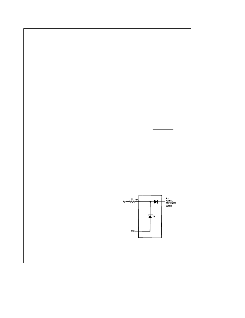
6.0 POWER SUPPLY
A unique feature of the ADC0833 is the inclusion of a 7V
zener diode connected from the V
a
terminal to ground
which also connects to the V
CC
terminal (which is the actual
converter supply) through a silicon diode, as shown in Fig-
ure 3.
TL/H/5607–8
FIGURE 3. An On-Chip Shunt Regulator Diode
12
相关PDF资料 |
PDF描述 |
|---|---|
| ADC0833CCJ | 8-Bit Serial I/O A/D Converter with 4-Channel Multiplexer |
| ADC0833CCN | 8-Bit Serial I/O A/D Converter with 4-Channel Multiplexer |
| ADC08351 | 8-Bit, 42 MSPS, 40 mW A/D Converter |
| ADC08351CIMTC | 8-Bit, 42 MSPS, 40 mW A/D Converter |
| ADC08351CIMTCX | 8-Bit, 42 MSPS, 40 mW A/D Converter |
相关代理商/技术参数 |
参数描述 |
|---|---|
| ADC0833BCN/A+ | 制造商:未知厂家 制造商全称:未知厂家 功能描述:Analog-to-Digital Converter, 8-Bit |
| ADC0833BCN/B+ | 制造商:未知厂家 制造商全称:未知厂家 功能描述:Analog-to-Digital Converter, 8-Bit |
| ADC0833CCJ | 制造商:NSC 制造商全称:National Semiconductor 功能描述:8-Bit Serial I/O A/D Converter with 4-Channel Multiplexer |
| ADC0833CCN | 制造商: 功能描述: 制造商:undefined 功能描述: |
| ADC0833CCN/A+ | 制造商:未知厂家 制造商全称:未知厂家 功能描述:Analog-to-Digital Converter, 8-Bit |
发布紧急采购,3分钟左右您将得到回复。