- 您现在的位置:买卖IC网 > PDF目录378279 > ADC08351CIMTC (NATIONAL SEMICONDUCTOR CORP) 8-Bit, 42 MSPS, 40 mW A/D Converter PDF资料下载
参数资料
| 型号: | ADC08351CIMTC |
| 厂商: | NATIONAL SEMICONDUCTOR CORP |
| 元件分类: | ADC |
| 英文描述: | 8-Bit, 42 MSPS, 40 mW A/D Converter |
| 中文描述: | 1-CH 8-BIT RESISTANCE LADDER ADC, PARALLEL ACCESS, PDSO20 |
| 封装: | TSSOP-20 |
| 文件页数: | 8/15页 |
| 文件大小: | 492K |
| 代理商: | ADC08351CIMTC |
Specification Definitions
(Continued)
FULL SCALE OFFSET ERROR
is the difference between
the analog input voltage that just causes the output code to
transition to the full scale code (all 1’s in the case of the
ADC08351) and the ideal value of 1
1
2
LSB below the value
of V
REF
.
INTEGRAL NON-LINEARITY (INL)
is a measure of the de-
viation of each individual code from a line drawn from zero
scale (
1
2
LSB below the first code transition) through positive
full scale (
1
2
LSB above the last code transition). The devia-
tion of any given code from this straight line is measured
from the center of that code value. The end point test method
is used.
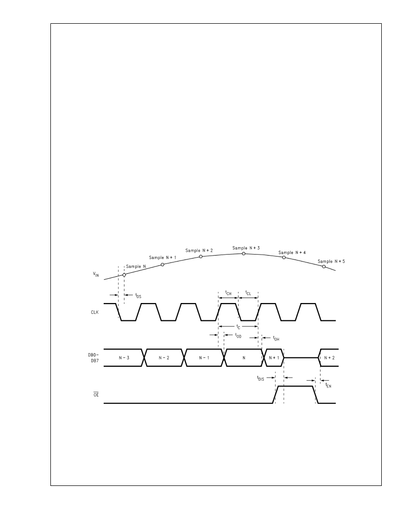
OUTPUT DELAY
is the time delay after the rising edge of
the input clock before the data update is present at the out-
put pins.
OUTPUT HOLD TIME
is the length of time that the output
data is valid after the rise of the input clock.
PIPELINE DELAY (LATENCY)
is the number of clock cycles
between initiation of conversion and the availability of that
conversion result at the output. New data is available at ev-
ery clock cycle, but the data lags the conversion by the pipe-
line delay.
SAMPLING (APERTURE) DELAY
is that time required after
the fall of the clock input for the sampling switch to open. The
sample is effectively taken this amount of time after the fall of
the clock input.
Timing Diagram
SIGNAL TO NOISE RATIO (SNR)
is the ratio of the rms
value of the input signal to the rms value of the other spectral
components below one-half the sampling frequency, not in-
cluding harmonics or dc.
SIGNAL TO NOISE PLUS DISTORTION (S/(N+D) or
SINAD)
is the ratio of the rms value of the input signal to the
rms value of all of the other spectral components below half
the clock frequency, including harmonics but excluding dc.
SPURIOUS FREE DYNAMIC RANGE (SFDR)
is the differ-
ence, expressed in dB, between the rms values of the input
signal and the peak spurious signal, where a spurious signal
is any signal present in the output spectrum that is not
present at the input.
TOTAL HARMONIC DISTORTION (THD)
is the ratio of the
rms total of the first six harmonic components to the rms
value of the input signal.
ZERO SCALE OFFSET ERROR
is the difference between
the analog input voltage that just causes the output code to
transition to the first code and the ideal value of
1
2
LSB for
that transition.
DS100895-23
FIGURE 1. ADC08351 Timing Diagram
A
www.national.com
8
相关PDF资料 |
PDF描述 |
|---|---|
| ADC08351CIMTCX | 8-Bit, 42 MSPS, 40 mW A/D Converter |
| ADC0841 | 8-Bit P Compatible A/D Converter |
| ADC0841BCN | 8-Bit P Compatible A/D Converter |
| ADC0841BCV | 8-Bit P Compatible A/D Converter |
| ADC0841CCN | 8-Bit P Compatible A/D Converter |
相关代理商/技术参数 |
参数描述 |
|---|---|
| ADC08351CIMTC/NOPB | 功能描述:IC ADC 8BIT 20-TSSOP RoHS:是 类别:集成电路 (IC) >> 数据采集 - 模数转换器 系列:- 产品培训模块:Lead (SnPb) Finish for COTS Obsolescence Mitigation Program 标准包装:2,500 系列:- 位数:12 采样率(每秒):3M 数据接口:- 转换器数目:- 功率耗散(最大):- 电压电源:- 工作温度:- 安装类型:表面贴装 封装/外壳:SOT-23-6 供应商设备封装:SOT-23-6 包装:带卷 (TR) 输入数目和类型:- |
| ADC08351CIMTCE/NOPB | 制造商:Texas Instruments 功能描述: |
| ADC08351CIMTCX | 功能描述:模数转换器 - ADC RoHS:否 制造商:Texas Instruments 通道数量:2 结构:Sigma-Delta 转换速率:125 SPs to 8 KSPs 分辨率:24 bit 输入类型:Differential 信噪比:107 dB 接口类型:SPI 工作电源电压:1.7 V to 3.6 V, 2.7 V to 5.25 V 最大工作温度:+ 85 C 安装风格:SMD/SMT 封装 / 箱体:VQFN-32 |
| ADC08351CIMTCX/NOPB | 功能描述:模数转换器 - ADC RoHS:否 制造商:Texas Instruments 通道数量:2 结构:Sigma-Delta 转换速率:125 SPs to 8 KSPs 分辨率:24 bit 输入类型:Differential 信噪比:107 dB 接口类型:SPI 工作电源电压:1.7 V to 3.6 V, 2.7 V to 5.25 V 最大工作温度:+ 85 C 安装风格:SMD/SMT 封装 / 箱体:VQFN-32 |
| ADC08351EVAL | 功能描述:EVALUATION BOARD FOR ADC08351 RoHS:是 类别:编程器,开发系统 >> 过时/停产零件编号 系列:- 标准包装:1 系列:- 传感器类型:CMOS 成像,彩色(RGB) 传感范围:WVGA 接口:I²C 灵敏度:60 fps 电源电压:5.7 V ~ 6.3 V 嵌入式:否 已供物品:成像器板 已用 IC / 零件:KAC-00401 相关产品:4H2099-ND - SENSOR IMAGE WVGA COLOR 48-PQFP4H2094-ND - SENSOR IMAGE WVGA MONO 48-PQFP |
发布紧急采购,3分钟左右您将得到回复。