- 您现在的位置:买卖IC网 > PDF目录378279 > ADC0848 (National Semiconductor Corporation) 8-Bit uP Compatible A/D Converters with Multiplexer Options PDF资料下载
参数资料
| 型号: | ADC0848 |
| 厂商: | National Semiconductor Corporation |
| 元件分类: | 串行ADC |
| 英文描述: | 8-Bit uP Compatible A/D Converters with Multiplexer Options |
| 中文描述: | 8位的兼容的A / D转换器和多路复用器选项 |
| 文件页数: | 4/20页 |
| 文件大小: | 467K |
| 代理商: | ADC0848 |
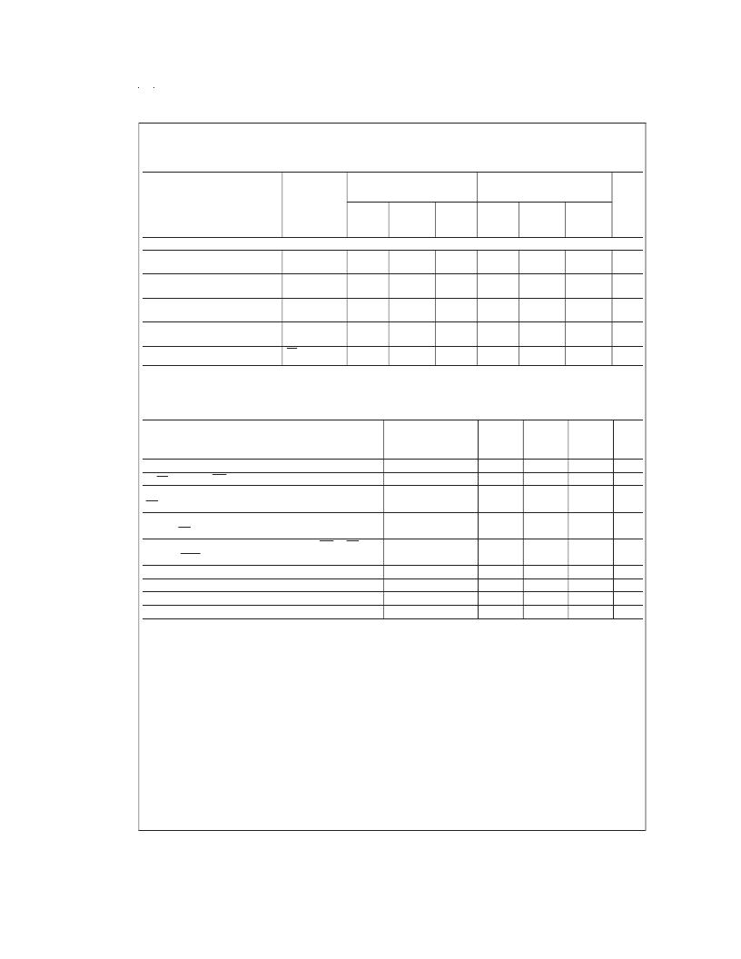
Electrical Characteristics
(Continued)
The following specifications apply for V
CC
= 5 V
DC
unless otherwise specified.
Boldface limits apply from T
MIN
to T
MAX
;
all
other limits T
A
= T
j
= 25C.
Parameter
Conditions
ADC0844BCJ
ADC0844CCJ
ADC0844CCN
ADC0848BCN, ADC0848CCN
ADC0848BCV, ADC0848CCV
Typ
Tested
(Note 5)
Limit
(Note 6)
Limit
Units
Typ
Tested
Limit
(Note 6)
Design
Limit
(Note 7)
Design
Limit
(Note 7)
(Note 5)
DIGITAL AND DC CHARACTERISTICS
V
OUT(0)
, Logical “0”
Output Voltage (Max)
I
OUT
, TRI-STATE Output
Current (Max)
I
SOURCE
, Output Source
Current (Min)
I
SINK
, Output Sink
Current (Min)
I
CC
, Supply Current (Max)
V
CC
=4.75V
I
OUT
=1.6 mA
V
OUT
=0V
V
OUT
=5V
V
OUT
=0V
0.4
0.34
0.4
V
0.01
0.01
14
3
3
6.5
0.01
0.01
14
0.3
0.3
7.5
3
3
6.5
μA
μA
mA
V
OUT
=V
CC
16
8.0
16
9.0
8.0
mA
CS =1, V
REF
Open
1
2.5
1
2.3
2.5
mA
AC Electrical Characteristics
The following specifications apply for V
CC
= 5V
DC
, t
r
= t
f
= 10 ns unless otherwise specified.
Boldface limits apply from T
MIN
to T
MAX
;
all other limits T
A
= T
j
= 25C.
Tested
Limit
(Note 6)
40
150
Design
Limit
(Note 7)
60
Parameter
Conditions
Typ
Units
(Note 5)
30
50
145
t
C
, Maximum Conversion Time (See Graph)
t
W(WR)
, Minimum WR Pulse Width
t
ACC
, Maximum Access Time (Delay from Falling Edge of
RD to Output Data Valid)
t
1H
, t
0H
, TRI-STATE Control (Maximum Delay from Rising
Edge of RD to Hi-Z State)
t
WI
, t
RI
, Maximum Delay from Falling Edge of WR or RD to
Reset of INTR
t
DS
, Minimum Data Set-Up Time
t
DH
, Minimum Data Hold Time
C
IN
, Capacitance of Logic Inputs
C
OUT
, Capacitance of Logic Outputs
μs
ns
ns
(Note 11)
C
L
= 100 pF
(Note 11)
C
L
= 10 pF, R
L
= 10k
(Note 11)
(Note 11)
225
125
200
ns
200
400
ns
(Note 11)
(Note 11)
50
0
5
5
100
50
ns
ns
pF
pF
Note 1:
Absolute Maximum Ratings indicate limits beyond which damage to the device may occur. DC and AC electrical specifications do not apply when operating
the device beyond its specified operating conditions.
Note 2:
All voltages are measured with respect to the ground pins.
Note 3:
When the input voltage (V
) at any pin exceeds the power supply rails (V
<
V
or V
>
V
+
) the absolute value of the current at that pin should be limited
to 5 mA or less. The 20 mA package input current limits the number of pins that can exceed the power supply boundaries with a 5 mA current limit to four.
Note 4:
Human body model, 100 pF discharged through a 1.5 k
resistor.
Note 5:
Typicals are at 25C and represent most likely parametric norm.
Note 6:
Tested limits are guaranteed to National’s AOQL (Average Outgoing Quality Level).
Note 7:
Design limits are guaranteed by not 100% tested. These limits are not used to calculate outgoing quality levels.
Note 8:
Total unadjusted error includes offset, full-scale, linearity, and multiplexer error.
Note 9:
For V
()
≥
V
(+) the digital output code will be 0000 0000. Two on-chip diodes are tied to each analog input, which will forward-conduct for analog input
voltages one diode drop below ground or one diode drop greater than V
supply. Be careful during testing at low V
levels (4.5V), as high level analog inputs (5V)
can cause this input diode to conduct, especially at elevated temperatures, and cause errors for analog inputs near full-scale. The spec allows 50 mV forward bias
of either diode. This means that as long as the analog V
does not exceed the supply voltage by more than 50 mV, the output code will be correct. To achieve an
absolute 0 V
DC
to 5 V
DC
input voltage range will therefore require a minimum supply voltage of 4.950 V
DC
over temperature variations, initial tolerance and loading.
Note 10:
Off channel leakage current is measured after the channel selection.
Note 11:
The temperature coefficient is 0.3%/C.
www.national.com
4
相关PDF资料 |
PDF描述 |
|---|---|
| ADC0848BCN | 8-Bit uP Compatible A/D Converters with Multiplexer Options |
| ADC0848BCV | 8-Bit uP Compatible A/D Converters with Multiplexer Options |
| ADC0848CCN | 8-Bit uP Compatible A/D Converters with Multiplexer Options |
| ADC0848CCV | 8-Bit uP Compatible A/D Converters with Multiplexer Options |
| ADC084S021 | 4 Channel, 200 kSPS, 12-Bit A/D Converter |
相关代理商/技术参数 |
参数描述 |
|---|---|
| ADC0848BCN | 制造商:NSC 制造商全称:National Semiconductor 功能描述:8-Bit uP Compatible A/D Converters with Multiplexer Options |
| ADC0848BCN/NOPB | 功能描述:IC ADC 8BIT MPU W/MUX OPT 24-DIP RoHS:是 类别:集成电路 (IC) >> 数据采集 - 模数转换器 系列:- 产品培训模块:Lead (SnPb) Finish for COTS Obsolescence Mitigation Program 标准包装:2,500 系列:- 位数:12 采样率(每秒):3M 数据接口:- 转换器数目:- 功率耗散(最大):- 电压电源:- 工作温度:- 安装类型:表面贴装 封装/外壳:SOT-23-6 供应商设备封装:SOT-23-6 包装:带卷 (TR) 输入数目和类型:- |
| ADC0848BCV | 功能描述:模数转换器 - ADC RoHS:否 制造商:Texas Instruments 通道数量:2 结构:Sigma-Delta 转换速率:125 SPs to 8 KSPs 分辨率:24 bit 输入类型:Differential 信噪比:107 dB 接口类型:SPI 工作电源电压:1.7 V to 3.6 V, 2.7 V to 5.25 V 最大工作温度:+ 85 C 安装风格:SMD/SMT 封装 / 箱体:VQFN-32 |
| ADC0848BCV/NOPB | 功能描述:模数转换器 - ADC RoHS:否 制造商:Texas Instruments 通道数量:2 结构:Sigma-Delta 转换速率:125 SPs to 8 KSPs 分辨率:24 bit 输入类型:Differential 信噪比:107 dB 接口类型:SPI 工作电源电压:1.7 V to 3.6 V, 2.7 V to 5.25 V 最大工作温度:+ 85 C 安装风格:SMD/SMT 封装 / 箱体:VQFN-32 |
| ADC0848BCVX | 功能描述:模数转换器 - ADC RoHS:否 制造商:Texas Instruments 通道数量:2 结构:Sigma-Delta 转换速率:125 SPs to 8 KSPs 分辨率:24 bit 输入类型:Differential 信噪比:107 dB 接口类型:SPI 工作电源电压:1.7 V to 3.6 V, 2.7 V to 5.25 V 最大工作温度:+ 85 C 安装风格:SMD/SMT 封装 / 箱体:VQFN-32 |
发布紧急采购,3分钟左右您将得到回复。