- 您现在的位置:买卖IC网 > PDF目录378279 > ADC0854CCN (NATIONAL SEMICONDUCTOR CORP) Multiplexed Comparator with 8-Bit Reference Divider PDF资料下载
参数资料
| 型号: | ADC0854CCN |
| 厂商: | NATIONAL SEMICONDUCTOR CORP |
| 元件分类: | ADC |
| 英文描述: | Multiplexed Comparator with 8-Bit Reference Divider |
| 中文描述: | 8-BIT COMPARATOR, ONE BIT ADC, SERIAL ACCESS, PDIP14 |
| 封装: | PLASTIC, DIP-14 |
| 文件页数: | 12/20页 |
| 文件大小: | 327K |
| 代理商: | ADC0854CCN |
Functional Description
(Continued)
2.0 THE DIGITAL INTERFACE
An important characteristic of the ADC0852 and ADC0854
is their serial data link with the controlling processor. A seri-
al communication format eliminates the transmission of low
level analog signals by locating the comparator close to the
signal source. Thus only highly noise immune digital signals
need to be transmitted back to the host processor.
To understand the operation of these devices it is best to
refer to the timing diagrams (Figure 3) and functional block
diagram (Figure 2) while following a complete comparison
sequence.
1. A comparison is initiated by first pulling the CS (chip se-
lect) line low. This line must be held low for the entire ad-
dressing sequence and comparison. The comparator then
waits for a start bit, its MUX assignment word, and an 8-bit
code to set the internal DAC which supplies the compara-
tor’s threshold voltage (V
TH
).
2. An external clock is applied to the CLK input. This clock
can be applied continuously and need not be gated on and
off.
3. On each rising edge of the clock, the level present on the
DI line is clocked into the MUX address shift register. The
start bit is the first logic ‘‘1’’ that appears on this line. All
leading zeroes are ignored. After the start bit, the ADC0852
expects the next 2 bits to be the MUX assignment word
while the ADC0854, with more MUX configurations, looks
for 3 bits.
4. Immediately after the MUX assignment word has been
clocked in, the shift register then reads the next eight bits as
the input code to the internal DAC. This eight bit word is
read LSB first and is used to set the voltage applied to the
comparator’s threshold input (internal).
5. After the rising edge of the 11th or 12th clock (ADC0852
or ADC0854 respectively) following the start bit, the com-
parator and DAC programming is complete. At this point the
DI line is disabled and ignores further inputs. Also at this
time the data out (DO) line comes out of TRI-STATE and
enters a don’t care state (undefined output) for 1.5 clock
cycles.
6. The result of the comparison between the programmed
threshold voltage and the difference between the two se-
lected inputs (V
IN
(
a
)
b
V
IN
(
b
)) is output to the DO line on
each subsequent high to low clock transition.
7. After programming, continuous comparison on the same
selected channel with the same programmed threshold can
be done indefinitely, without reprogramming the device, as
long as CS remains low. Each new comparator decision will
be shifted to the output on the falling edge of the clock.
However, the output will, in effect, ‘‘lag’’ the analog input by
0.5 to 1.5 clock cycles because of the time required to make
the comparison and latch the output (see Figure 5).
8. All internal registers are cleared when the CS line is
brought high. If another comparison is desired CS must
make a high to low transition followed by new address and
threshold programming.
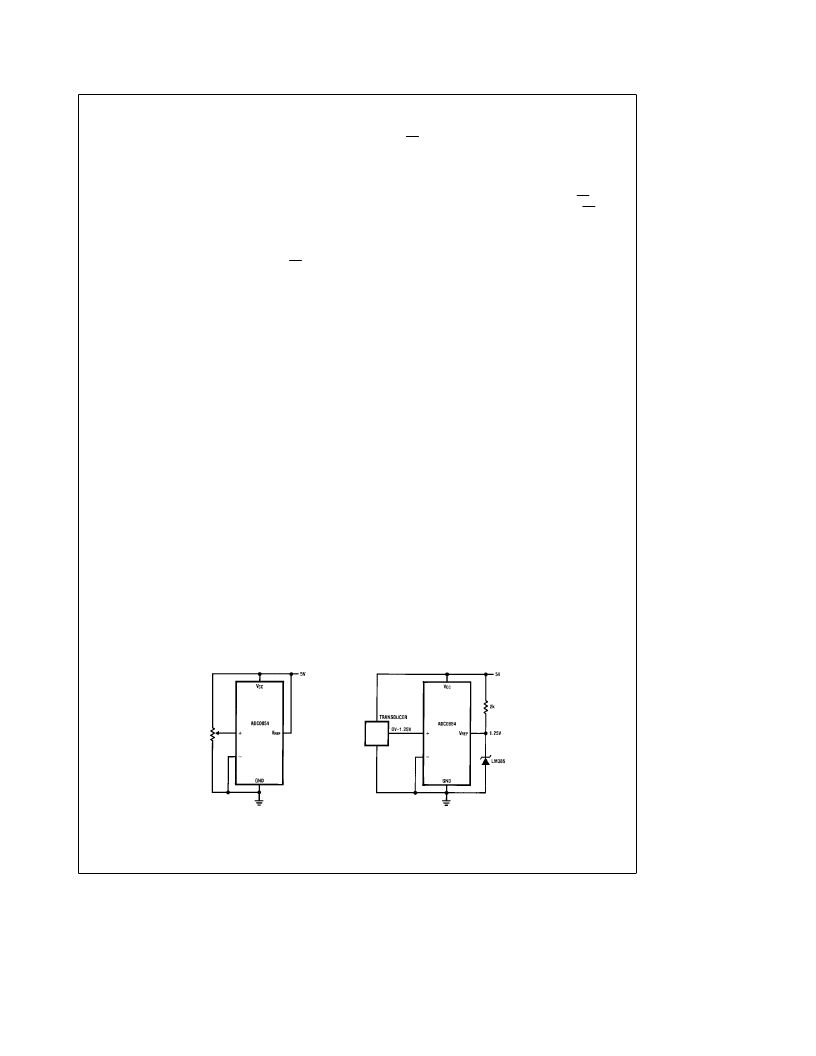
3.0 REFERENCE CONSIDERATIONS / RATIOMETRIC
OPERATION
The voltage applied to the ‘‘V
REF
’’ input of the DAC defines
the voltage span that can be programmed to appear at the
threshold input of the comparator. The ADC0854 can be
used in either ratiometric applications or in systems with
absolute references. The V
REF
pin must be connected to a
source capable of driving the DAC ladder resistance (typ.
2.4 k
X
) with a stable voltage.
In ratiometric systems, the analog input voltage is normally
a proportion of the DAC’s or A/D’s reference voltage. For
example, a mechanical position servo using a potentiometer
to indicate rotation, could use the same voltage to drive the
reference as well as the potentiometer. Changes in the val-
ue of V
REF
would not affect system accuracy since only the
relative value of these signals to each other is important.
This technique relaxes the stability requirements of the sys-
tem reference since the analog input and DAC reference
move together, thus maintaining the same comparator out-
put for a given input condition.
In the absolute case, the V
REF
input can be driven with a
stable voltage source whose output is insensitive to time
and temperature changes. The LM385 and LM336 are good
low current devices for this purpose.
The maximum value of V
REF
is limited to the V
CC
supply
voltage. The minimum value can be quite small (see typical
performance curves) allowing the effective resolution of the
comparator threshold DAC to also be small (V
REF
e
0.5V,
DAC resolution
e
2.0 mV). This in turn lets the designer
have finer control over the comparator trip point. In such
instances however, more care must be taken with regard to
noise pickup, grounding, and system error sources.
TL/H/5521–16
a) Ratiometric
b) Absolute with a Reduced Span
FIGURE 7. Referencing Examples
12
相关PDF资料 |
PDF描述 |
|---|---|
| ADC0852 | Synchronous 4-Bit Up/Down Counters With Up/Down Mode Control 16-PDIP 0 to 70 |
| ADC0852CCN | Multiplexed Comparator with 8-Bit Reference Divider |
| ADC0858BIN | 8-Bit Analog Data Acquisition and Monitoring Systems |
| ADC0858BIV | 8-Bit Analog Data Acquisition and Monitoring Systems |
| ADC0851 | 8-Bit Analog Data Acquisition and Monitoring Systems |
相关代理商/技术参数 |
参数描述 |
|---|---|
| ADC0854CCN/A+ | 制造商:未知厂家 制造商全称:未知厂家 功能描述:Analog Comparator |
| ADC0854CCN/B+ | 制造商:未知厂家 制造商全称:未知厂家 功能描述:Analog Comparator |
| ADC0858 | 制造商:未知厂家 制造商全称:未知厂家 功能描述: |
| ADC0858BIJ | 制造商:未知厂家 制造商全称:未知厂家 功能描述:Single-Ended Data Acquisition System |
| ADC0858BIN | 制造商:NSC 制造商全称:National Semiconductor 功能描述:8-Bit Analog Data Acquisition and Monitoring Systems |
发布紧急采购,3分钟左右您将得到回复。