- 您现在的位置:买卖IC网 > PDF目录378279 > ADC0858BIN (NATIONAL SEMICONDUCTOR CORP) 8-Bit Analog Data Acquisition and Monitoring Systems PDF资料下载
参数资料
| 型号: | ADC0858BIN |
| 厂商: | NATIONAL SEMICONDUCTOR CORP |
| 元件分类: | ADC |
| 英文描述: | 8-Bit Analog Data Acquisition and Monitoring Systems |
| 中文描述: | 8-CH 8-BIT SUCCESSIVE APPROXIMATION ADC, SERIAL ACCESS, PDIP20 |
| 封装: | PLASTIC, DIP-20 |
| 文件页数: | 25/36页 |
| 文件大小: | 581K |
| 代理商: | ADC0858BIN |
第1页第2页第3页第4页第5页第6页第7页第8页第9页第10页第11页第12页第13页第14页第15页第16页第17页第18页第19页第20页第21页第22页第23页第24页当前第25页第26页第27页第28页第29页第30页第31页第32页第33页第34页第35页第36页
3.0 Watchdog Mode
(Continued)
TL/H/11021–48
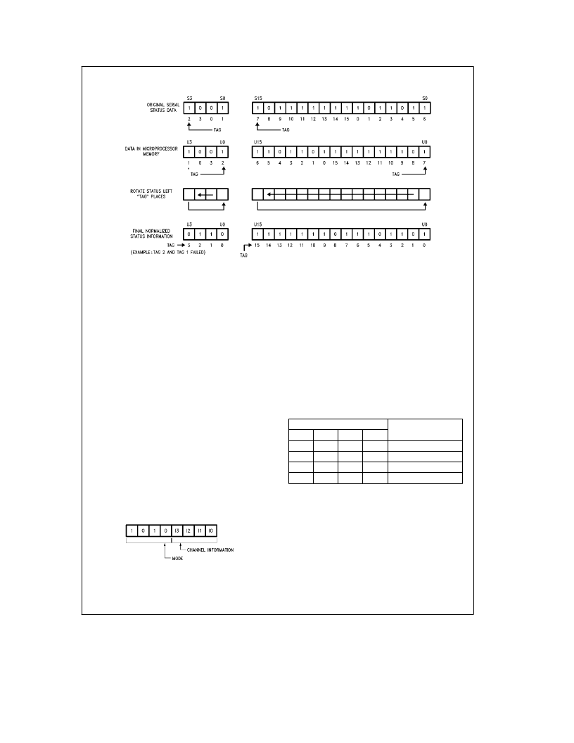
FIGURE 9. Status Bit Normalization
4.0 A/D Conversion Modes
The ADC0851/8 can be used in two A/D conversion
modes. In ‘‘One A/D conversion’’ mode, the device oper-
ates as a multiplexed A/D converter and a conversion may
be initiated on any channel or channel pair configured in the
differential mode. In the ‘‘Automatic A/D conversion’’ mode,
an A/D conversion is done on a channel or channel pair and
after the output data is transmitted, conversion begins on
the next subsequent channel or channel pair. This process
will continue unless the device’s mode of operation is
changed.
Note that the A/D conversion time is determined by the
oscillator clock period and has no relation with the digital
clock signal, CLK. The oscillator clock’s frequency is set by
connecting a resistor from the OSC pin (pin 2 for ADC0851
or ADC0858) to V
CC
and a capacitor from the OSC pin to
ground. The conversion time of the A/D converter is eigh-
teen OSC clock periods maximum. Assuming that the oscil-
lation clock frequency is set at 1 MHz (with R
ext
e
3.16 k
X
and C
ext
e
170 pF) then the conversion time would be
18
m
s maximum.
4.1 ONE A/D CONVERSION MODE
This mode is used to initiate one A/D conversion on a single
channel or channel pair configured in the differential mode.
The necessary mode address as per Table I is 1 0 1 0. The
format for the input word is as follows:
Data Input (DI) wordDADC0851 or ADC0858.
TL/H/11021–49
(Table V(a) for ADC0851, Table V(b) for ADC0858)
The 4-bit data following the mode address is the channel
information address. These four bits assign the MUX config-
uration for the single A/D conversion. The channel informa-
tion addresses and the corresonding MUX configurations
are shown in Table V(a) and (b) for ADC0851 and ADC0858
respectively. Note that the ADC0851 only decodes the two
LSBs of the channel information data while ignoring the two
MSBs (I3 and I2). When a channel pair is configured in the
differential mode, it is important to note that the arithmetic
difference of the channel voltages should not be negative.
Negative difference voltage would result in all zeroes at the
output.
TABLE V(a). Channel Information for
One A/D Conversion (ADC0851)
Channel Information
Channels Enabled
I3
I2
I1
I0
X
X
0
0
CH0
X
X
0
1
CH0–CH1
X
X
1
0
CH1
X
X
1
1
Invalid
25
相关PDF资料 |
PDF描述 |
|---|---|
| ADC0858BIV | 8-Bit Analog Data Acquisition and Monitoring Systems |
| ADC0851 | 8-Bit Analog Data Acquisition and Monitoring Systems |
| ADC0851BIN | 8-Bit Analog Data Acquisition and Monitoring Systems |
| ADC0851BIV | 8-Bit Analog Data Acquisition and Monitoring Systems |
| ADC0851CIN | 8-Bit Analog Data Acquisition and Monitoring Systems |
相关代理商/技术参数 |
参数描述 |
|---|---|
| ADC0858BIV | 制造商:NSC 制造商全称:National Semiconductor 功能描述:8-Bit Analog Data Acquisition and Monitoring Systems |
| ADC0858CIJ | 制造商:未知厂家 制造商全称:未知厂家 功能描述:Single-Ended Data Acquisition System |
| ADC0858CIN | 制造商:NSC 制造商全称:National Semiconductor 功能描述:8-Bit Analog Data Acquisition and Monitoring Systems |
| ADC0858CIV | 制造商:NSC 制造商全称:National Semiconductor 功能描述:8-Bit Analog Data Acquisition and Monitoring Systems |
| ADC0858CMJ/883 | 制造商:未知厂家 制造商全称:未知厂家 功能描述:Single-Ended Data Acquisition System |
发布紧急采购,3分钟左右您将得到回复。