- 您现在的位置:买卖IC网 > PDF目录378280 > ADC08831 (National Semiconductor Corporation) Synchronous 4-Bit Up/Down Binary Counters With Dual Clock and Clear 16-SOIC 0 to 70 PDF资料下载
参数资料
| 型号: | ADC08831 |
| 厂商: | National Semiconductor Corporation |
| 元件分类: | 通用总线功能 |
| 英文描述: | Synchronous 4-Bit Up/Down Binary Counters With Dual Clock and Clear 16-SOIC 0 to 70 |
| 中文描述: | 8位串行I / O的CMOS的A / D转换器多路复用器和采样/保持功能 |
| 文件页数: | 5/23页 |
| 文件大小: | 486K |
| 代理商: | ADC08831 |
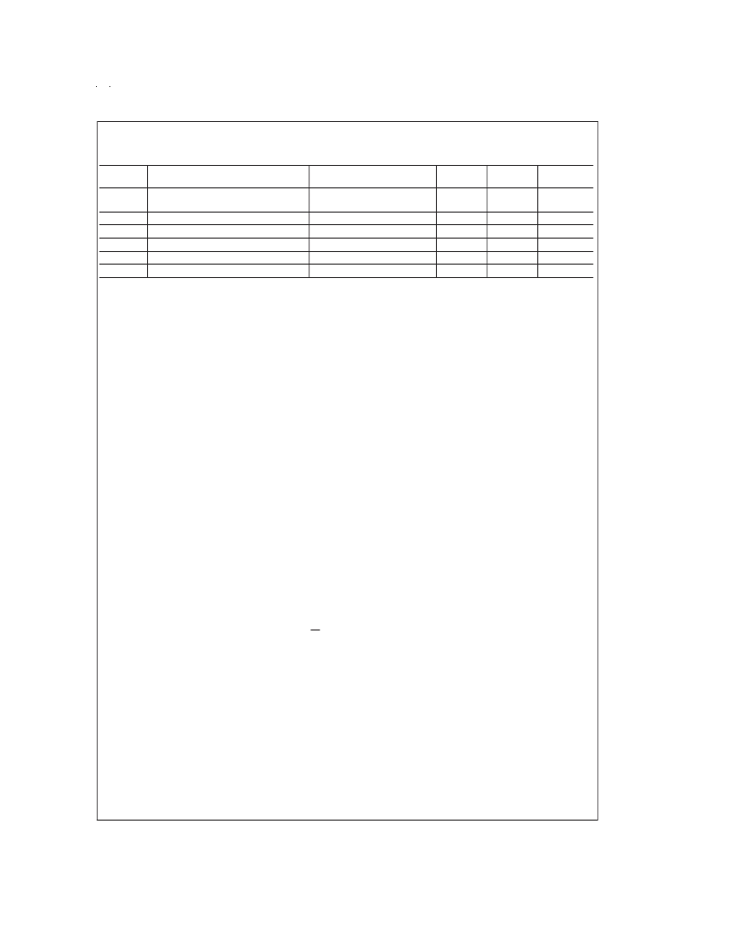
Dynamic Characteristics
The following specifications apply for V
= 5V, f
CLK
= 2MHz, T
A
= 25C, R
SOURCE
= 50
, f
IN
= 45kHz, V
IN
= 5V
P
, V
REF
= 5V,
non-coherent 2048 samples with windowing.
Symbol
Parameter
Conditions
Typical
(Note 8)
Limits
(Note 9)
181
153
Units
(Limits)
ksps
ksps
dB
dB
dB
Bits
dB
f
S
Sampling Rate
ADC08831
ADC08832
f
CLK
/11
f
CLK
/13 (Note 21)
SNR
THD
SINAD
ENOB
SFDR
Signal-to -Noise Ratio (Note 19)
Total Harmonic Distortion (Note 20)
Signal-to -Noise and Distortion
Effective Number Of Bits (Note 18)
Spurious Free Dynamic Range
48.5
59.5
48.0
7.7
62.5
Note 1:
Absolute Maximum Ratings indicate limits beyond which damage to the device may occur.
Note 2:
Operating Ratings indicate conditions for which the device is functional. These ratings do not guarantee specific performance limits. For guaranteed speci-
fications and test conditions, see the Electrical Characteristics. The guaranteed specifications apply only for the test conditions listed. Some performance character-
istics may degrade when the device is not operated under the listed test conditions.
Note 3:
All voltages are measured with respect to GND = 0 V
DC
, unless otherwise specified.
Note 4:
When the input voltage V
at any pin exceeds the power supplies (V
<
(GND) or V
>
V
,) the current at that pin should be limited to 5 mA. The 20
mA maximum package input current rating limits the number of pins that can safely exceed the power supplies with an input current of 5 mA to four pins.
Note 5:
The maximum power dissipation must be derated at elevated temperatures and is dictated by T
,
θ
and the ambient temperature, T
. The maximum
allowable power dissipation at any temperature is P
D
= (T
JMAX
T
A
)/
θ
JA
or the number given in the Absolute Maximum Ratings, whichever is lower.
Note 6:
Human body model, 100 pF capacitor discharged through a 1.5 k
resistor. The machine mode is a 200pF capacitor discharged directly into each pin.
Note 7:
See AN450 “Surface Mounting Methods and Their Effect on Product Reliability” or Linear Data Book section “Surface Mount” for other methods of soldering
surface mount devices.
Note 8:
Typicals are at T
J
= 25C and represent the most likely parametric norm.
Note 9:
Guaranteed to National’s AOQL (Average Outgoing Quality Level).
Note 10:
Total Unadjusted Error (TUE) includes offset, full-scale, linearity, multiplexer errors.
Note 11:
It is not tested for the ADC08832.
Note 12:
For V
≥
V
the digital code will be 0000 0000. Two on-chip diodes are tied to each analog input (see Functional Block Diagram) which will
forward-conduct for analog input voltages one diode drop below ground or one diode drop greater than V
supply. During testing at low V
levels (e.g., 4.5V), high
level analog inputs (e.g., 5V) can cause an input diode to conduct, especially at elevated temperatures, which will cause errors for analog inputs near full-scale. The
spec allows 50 mV forward bias of either diode; this means that as long as the analog V
does not exceed the supply voltage by more than 50 mV, the output code
will be correct. Exceeding this range on an unselected channel will corrupt the reading of a selected channel.Achievement of an absolute 0 V
DC
to 5 V
DC
input voltage
range will therefore require a minimum supply voltage of 4.950 V
DC
over temperature variations, initial tolerance and loading.
Note 13:
Channel leakage current is measured after a single-ended channel is selected and the clock is turned off. For off channel leakage current the following two
cases are considered: one, with the selected channel tied high (5 V
) and the remaining off channel tied low (0 V
), total current flow through the off channel is
measured; two, with the selected channel tied low and the off channels tied high, total current flow through the off channel is again measured. The two cases con-
sidered for determining on channel leakage current are the same except total current flow through the selected channel is measured.
Note 14:
A 40% to 60% duty cycle range insures proper operation at all clock frequencies. In the case that an available clock has a duty cycle outside of these limits
the minimum time the clock is high or low must be at least 250 ns. The maximum time the clock can be high or low is 60 μs.
Note 15:
Since data, MSB first, is the output of the comparator used in the successive approximation loop, an additional delay is built in to allow for comparator re-
sponse time.
Note 16:
For the ADC08832 V
ref
is internally tied to V
CC
, therefore, for the ADC08832 reference current is included in the supply current.
Note 17:
Analog inputs are typically 300 ohms input resistance to a 13pF sample and hold capacitor.
Note 18:
Effective Number Of Bits (ENOB) is calculated from the measured signal-to-noise plus distortion ratio (SINAD) using the equation ENOB = (SINAD-1.76)/
6.02.
Note 19:
The signal-to-noise ratio is the ratio of the signal amplitude to the background noise level. Harmonics of the input signal are not included in it’s calculation.
Note 20:
The contributions from the first 6 harmonics are used in the calculation of the THD.
Note 21:
The maximum sampling rate is slightly less than f
CLK
/11 if CS is reset in less than one clock period.
www.national.com
5
相关PDF资料 |
PDF描述 |
|---|---|
| ADC08832IM | 8-Bit Serial I/O CMOS A/D Converters with Multiplexer and Sample/Hold Function |
| ADC08832IMM | Synchronous 4-Bit Up/Down Binary Counters With Dual Clock and Clear 16-SOIC 0 to 70 |
| ADC08832IN | Synchronous 4-Bit Up/Down Binary Counters With Dual Clock and Clear 16-SOIC 0 to 70 |
| ADC08831IM | 8-Bit Serial I/O CMOS A/D Converters with Multiplexer and Sample/Hold Function |
| ADC08831IMM | 8-Bit Serial I/O CMOS A/D Converters with Multiplexer and Sample/Hold Function |
相关代理商/技术参数 |
参数描述 |
|---|---|
| ADC08831IM | 功能描述:模数转换器 - ADC RoHS:否 制造商:Texas Instruments 通道数量:2 结构:Sigma-Delta 转换速率:125 SPs to 8 KSPs 分辨率:24 bit 输入类型:Differential 信噪比:107 dB 接口类型:SPI 工作电源电压:1.7 V to 3.6 V, 2.7 V to 5.25 V 最大工作温度:+ 85 C 安装风格:SMD/SMT 封装 / 箱体:VQFN-32 |
| ADC08831IM/NOPB | 功能描述:模数转换器 - ADC RoHS:否 制造商:Texas Instruments 通道数量:2 结构:Sigma-Delta 转换速率:125 SPs to 8 KSPs 分辨率:24 bit 输入类型:Differential 信噪比:107 dB 接口类型:SPI 工作电源电压:1.7 V to 3.6 V, 2.7 V to 5.25 V 最大工作温度:+ 85 C 安装风格:SMD/SMT 封装 / 箱体:VQFN-32 |
| ADC08831IM/NOPB | 制造商:Texas Instruments 功能描述:A/D Converter (A-D) IC |
| ADC08831IMM | 制造商:NSC 制造商全称:National Semiconductor 功能描述:8-Bit Serial I/O CMOS A/D Converters with Multiplexer and Sample/Hold Function |
| ADC08831IMM/NOPB | 功能描述:IC ADC 8BIT SERIAL I/O 8-MSOP RoHS:是 类别:集成电路 (IC) >> 数据采集 - 模数转换器 系列:- 产品培训模块:Lead (SnPb) Finish for COTS Obsolescence Mitigation Program 标准包装:2,500 系列:- 位数:12 采样率(每秒):3M 数据接口:- 转换器数目:- 功率耗散(最大):- 电压电源:- 工作温度:- 安装类型:表面贴装 封装/外壳:SOT-23-6 供应商设备封装:SOT-23-6 包装:带卷 (TR) 输入数目和类型:- |
发布紧急采购,3分钟左右您将得到回复。