- 您现在的位置:买卖IC网 > PDF目录378280 > ADC10030CIVT (NATIONAL SEMICONDUCTOR CORP) 10-Bit, 30 MSPS, 125 mW A/D Converter with Internal Sample and Hold PDF资料下载
参数资料
| 型号: | ADC10030CIVT |
| 厂商: | NATIONAL SEMICONDUCTOR CORP |
| 元件分类: | ADC |
| 英文描述: | 10-Bit, 30 MSPS, 125 mW A/D Converter with Internal Sample and Hold |
| 中文描述: | 1-CH 10-BIT RESISTANCE LADDER ADC, PARALLEL ACCESS, PQFP32 |
| 封装: | TQFP-32 |
| 文件页数: | 7/17页 |
| 文件大小: | 417K |
| 代理商: | ADC10030CIVT |
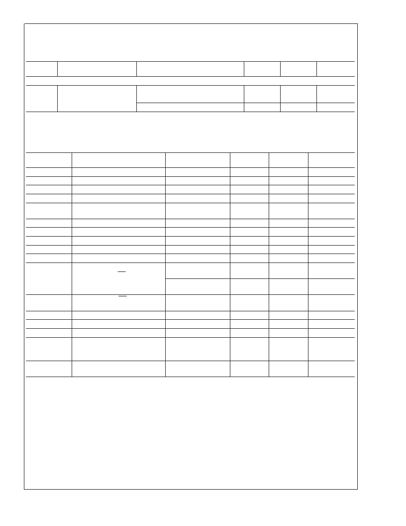
Reference, DC, and Logic Electrical Characteristics
(Continued)
The following specifications apply for V
= +5.0V
DC
, V
= +5.0V
, V
I/O = +5.0V
DC
, V
REF
+ = +3.5V
, V
=
+1.75V
DC
, C
L
= 20 pF, f
CLK
= 27 MHz, R
S
= 50
.
Boldface limits apply for T
A
= T
MIN
MAX
:
all other limits T
A
= 25C
(Note 7)
Symbol
Parameter
Conditions
Typical
(Note 8)
Limits
(Note 9)
Units
Power Supply Characteristics
P
D
Power Consumption
PD = LOW
PD = HIGH
PD = LOW, f
CLK
= 30 MHz
121
3.5
125
130
mW(max)
mW
AC Electrical Characteristics
The following specifications apply for V
= +5.0V
DC
, V
= +5.0V
, V
I/O = 5.0V
, V
REF
+ = +3.5V
, V
=
+1.75V
DC
, C
L
= 20 pF, f
CLK
= 27 MHz, R
S
= 50
.
Boldface limits apply for T
A
= T
MIN
MAX
:
all other limits T
A
= 25C
(Note 7)
Symbol
Parameter
Conditions
Typical
(Note 8)
27
1
Limits
(Note 9)
30
Units
(Limits)
MHz
MHz
ns(min)
ns(min)
%(min)
%(max)
Clock Cycles
ns(max)
ns
ns(max)
ns
f
CLK1
f
CLK2
t
CH
t
CL
Maximum Clock Frequency
Minimum Clock Frequency
Clock High Time
Clock Low Time
16.5
16.5
45
55
2.0
4
Duty Cycle
50
Pipeliine Delay (Latency)
Clock Input Rise and Fall Time
Output Rise and Fall Times
Fall of CLK to Data Valid
Output Data Hold Time
t
rc
, t
fc
t
r
, t
f
t
OD
t
OH
10
20
12
25
t
DIS
Rising Edge of OE to
TRI-STATE
From Output High,
2 k
to Ground
From Output Low, 2
k
to V
D
I/O
25
ns
18
ns
t
EN
Falling Edge of OE to Valid
Data
Data Valid Time
Aperture Jitter
Full Scale Step Response
1 k
to V
CC
25
ns
t
VALID
t
AJ
27
<
30
1
ns
ps
t
r
= 10 ns
V
IN
Step from
(V
REF
+ +100 mV) to
(V
REF
)
conversion
Overrange Recovery Time
1
conversion
t
WU
PD Low to
1
2
LSB Accurate
Conversion (Wake-Up Time)
700
ns
Note 1:
Absolute Maximum Ratings indicate limits beyond which damage to the device may occur. Operating Ratings indicate conditions for which the device is func-
tional, but do not guarantee specific performance limits. For guaranteed specifications and test conditions, see the Electrical Characteristics. The guaranteed speci-
fications apply only for the test conditions listed. Some performance characteristics may degrade when the device is not operated under the listed test conditions.
Note 2:
All voltages are measured with respect to GND = AGND = DGND = 0V, unless otherwise specified.
Note 3:
When the input voltage at any pin exceeds the power supplies (V
<
GND or V
>
V
or V
), the current at that pin should be limited to 25 mA. The 50 mA
maximum package input current rating limits the number of pins that can safely exceed the power supplies with an input current of 25 mA to two.
Note 4:
The absolute maximum junction temperature (T
max) for this device is 150C. The maximum allowable power dissipation is dictated by T
max, the
junction-to-ambient thermal resistance (
θ
), and the ambient temperature (T
), and can be calculated using the formula P
MAX = (T
max T
)/
θ
. In the 32-pin
TQFP,
θ
is 69C/W, so P
MAX = 1,811 mW at 25C and 942 mW at the maximum operating ambient temperature of 85C. Note that the power dissipation of this
device under normal operation will typically be about 137 mW (125 mW quiescent power + 2 mW reference ladder power +10 mW due to 1 TTL load on each digital
output). The values for maximum power dissipation listed above will be reached only when the ADC10030 is operated in a severe fault condition (e.g. when input or
output pins are driven beyond the power supply voltages, or the power supply polarity is reversed). Obviously, such conditions should always be avoided.
Note 5:
Human body model is 100 pF capacitor discharged through a 1.5 k
resistor. Machine model is 220 pF discharged through ZERO
.
Note 6:
See AN450, “Surface Mounting Methods and Their Effect on Product Reliability”, or the section entitled “Surface Mount” found in any post 1986 National
Semiconductor Linear Data Book, for other methods of soldering surface mount devices.
Note 7:
The inputs are protected as shown below. Input voltage magnitudes up to 300 mV beyond the supply rails will not damage this device. However, errors in
the A/D conversion can occur if the input goes above V
A
or below AGND by more than 300 mV.
A
www.national.com
7
相关PDF资料 |
PDF描述 |
|---|---|
| ADC10030 | 10-Bit, 30 MSPS, 125 mW A/D Converter with Internal Sample and Hold |
| ADC10040 | ECONOLINE: REC3-S_DRW(Z)/H4,H6 - Safety standards and approval: EN 60950 certified, rated for 250VAV (LVD test report)- Applied for Ul 1950 Component Recognised Certification- 3W DIP Package- 4kVDC & 6kVDC Isolation- Regulated Output- Continuous Short Circiut Protection Auto-Restarting |
| ADC10040CIMT | 10-Bit, 40 MSPS, 3V, 55.5 mW A/D Converter |
| ADC10040CIMTX | 10-Bit, 40 MSPS, 3V, 55.5 mW A/D Converter |
| ADC1005 | 10-BIT uP COMPATIBLE A/D CONVERTERS |
相关代理商/技术参数 |
参数描述 |
|---|---|
| ADC10030CIVT/NOPB | 功能描述:IC ADC 10BIT 32-LQFP RoHS:是 类别:集成电路 (IC) >> 数据采集 - 模数转换器 系列:- 产品培训模块:Lead (SnPb) Finish for COTS Obsolescence Mitigation Program 标准包装:2,500 系列:- 位数:12 采样率(每秒):3M 数据接口:- 转换器数目:- 功率耗散(最大):- 电压电源:- 工作温度:- 安装类型:表面贴装 封装/外壳:SOT-23-6 供应商设备封装:SOT-23-6 包装:带卷 (TR) 输入数目和类型:- |
| ADC10030EVAL | 功能描述:BOARD EVALUATION FOR ADC10030 RoHS:是 类别:编程器,开发系统 >> 过时/停产零件编号 系列:- 标准包装:1 系列:- 传感器类型:CMOS 成像,彩色(RGB) 传感范围:WVGA 接口:I²C 灵敏度:60 fps 电源电压:5.7 V ~ 6.3 V 嵌入式:否 已供物品:成像器板 已用 IC / 零件:KAC-00401 相关产品:4H2099-ND - SENSOR IMAGE WVGA COLOR 48-PQFP4H2094-ND - SENSOR IMAGE WVGA MONO 48-PQFP |
| ADC1003S030 | 制造商:PHILIPS 制造商全称:NXP Semiconductors 功能描述:Single 10 bits ADC, up to 30 MHz, 40 MHz or 50 MHz, with voltage regulator |
| ADC1003S030/DB | 功能描述:数据转换 IC 开发工具 ADC DEMO BOARD RoHS:否 制造商:Texas Instruments 产品:Demonstration Kits 类型:ADC 工具用于评估:ADS130E08 接口类型:SPI 工作电源电压:- 6 V to + 6 V |
| ADC1003S030-DB | 功能描述:数据转换 IC 开发工具 RoHS:否 制造商:Texas Instruments 产品:Demonstration Kits 类型:ADC 工具用于评估:ADS130E08 接口类型:SPI 工作电源电压:- 6 V to + 6 V |
发布紧急采购,3分钟左右您将得到回复。