- 您现在的位置:买卖IC网 > PDF目录378281 > ADC10158CIN (NATIONAL SEMICONDUCTOR CORP) 10-Bit Plus Sign 4 レs ADCs with 4- or 8-Channel MUX, Track/Hold and Reference PDF资料下载
参数资料
| 型号: | ADC10158CIN |
| 厂商: | NATIONAL SEMICONDUCTOR CORP |
| 元件分类: | ADC |
| 英文描述: | 10-Bit Plus Sign 4 レs ADCs with 4- or 8-Channel MUX, Track/Hold and Reference |
| 中文描述: | 8-CH 10-BIT SUCCESSIVE APPROXIMATION ADC, PARALLEL ACCESS, PDIP28 |
| 封装: | DIP-28 |
| 文件页数: | 16/23页 |
| 文件大小: | 439K |
| 代理商: | ADC10158CIN |
1.0 Functional Description
The ADC10154 and ADC10158 use successive approxima-
tion to digitize an analog input voltage. Additional logic has
been incorporated in the devices to allow for the programma-
bility of the resolution, conversion time and digital output for-
mat. A capacitive array and a resistive ladder structure are
used in the DAC portion of the A/D converters. The structure
of the DAC allows a very simple switching scheme to provide
a very versatile analog input multiplexer. Also, inherent in
this structure is a sample/hold. A 2.5V CMOS band-gap ref-
erence is also provided on the ADC10154 and ADC10158.
1.1 DIGITAL INTERFACE
The ADC10154 and ADC10158 have eight digital outputs
(DB0–DB8) and can be easily interfaced to an 8-bit data
bus. Taking CS and WR low simultaneously will strobe the
data word on the data-bus into the input latch. This word will
be decoded to determine the multiplexer channel selection,
the A/D conversion resolution and the output data format.
The following table shows the input word data-bit assign-
ment.
DB0 through DB4 are assigned to the multiplexer address
data bits zero through four (MA0–MA4). Tables 2, 3describe
the multiplexer address assignment. DB5 selects unsigned
or signed (U/S) operation. DB6 selects 8- or 10-bit resolu-
tion. DB7 selects left or right justification of the output data.
Refer to Table 1 for the effect the Control Input Data has on
the digital output word.
The conversion process is started by the rising edge of WR,
which sets the “start conversion” bit inside theADC. If this bit
is set, the converter will start acquiring the input voltage on
the next falling edge of the internal CLK
÷
2 signal. The acqui-
sition period is 3 CLK
÷
2 periods, or 6 CLK periods. Immedi-
ately after the acquisition period the input signal is held and
the actual conversion begins. The number of clocks required
for a conversion is given in the following table:
Conversion Type
CLK
÷
2
Cycles
CLK
Cycles (N)
16
18
20
22
8-Bit
8-Bit + Sign
10-Bit
10-Bit + Sign
Since the CLK
÷
2 signal is internal to the ADC, it is initially
impossible to know which falling edge of CLK corresponds to
the falling edge of CLK
÷
2. For the first conversion, the rising
edge of WR should occur at least t
ns before any falling
edge of CLK. If this edge happens to be on the rising edge of
CLK
÷
2, this will add 2 CLK cycles to the total conversion
time. The phase of the CLK
÷
2 signal can be determined at
the end of the first conversion, when INT goes low. INT al-
ways goes low on the falling edge of the CLK
÷
2 signal. From
the first falling edge of INT onward, every other falling edge
of CLK will correspond to the falling edge of CLK
÷
2. With the
phase of CLK
÷
2 now known, the conversion time can be
minimized by taking WR high at least t
WS
ns before the fall-
ing edge of CLK
÷
2.
Upon completion of the conversion, INT goes low to signal
the A/D conversion result is ready to be read. Taking CS and
RD low will enable the digital output buffer and put byte 1 of
the conversion result on DB0 through DB7. The falling edge
of RD resets the INT output high. Taking CS and RD low a
second time will put byte 2 of the conversion result on
DB7–DB0. Table 1defines the DB0–DB7 assignment for dif-
ferent Control Input Data. The second read does not have to
be completed before a new conversion is started.
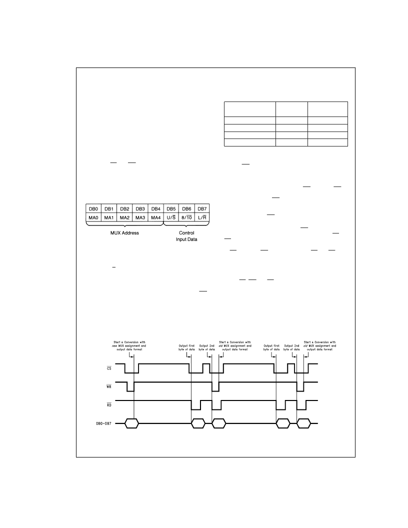
Taking CS, WR and RD low simultaneously will start a con-
version without changing the multiplexer channel assign-
ment or output configuration and resolution. The timing dia-
gram in Figure 3 shows the sequence of events that
implement this function. Refer to Diagrams 1, 2, and 3 in the
Timing Diagrams section for the timing constraints that must
be met.
8
9
10
11
DS011225-44
DS011225-19
FIGURE 3. Starting a Conversion without Updating the Channel Configuration, Resolution, or Data Format
A
www.national.com
16
相关PDF资料 |
PDF描述 |
|---|---|
| ADC1021 | 10-BIT uP COMPATIBLKE A/D CONVERTERS |
| ADC1021CCJ | 10-BIT uP COMPATIBLKE A/D CONVERTERS |
| ADC1021CCJ-1 | 10-BIT uP COMPATIBLKE A/D CONVERTERS |
| ADC10221CIVT | 10-Bit, 15 MSPS, 98 mW A/D Converter with Internal Sample and Hold |
| ADC10221 | 10-Bit, 15 MSPS, 98 mW A/D Converter with Internal Sample and Hold |
相关代理商/技术参数 |
参数描述 |
|---|---|
| ADC10158CIN/NOPB | 功能描述:IC ADC 10BIT W/4-8 CH MX 28-DIP RoHS:是 类别:集成电路 (IC) >> 数据采集 - 模数转换器 系列:- 产品培训模块:Lead (SnPb) Finish for COTS Obsolescence Mitigation Program 标准包装:2,500 系列:- 位数:12 采样率(每秒):3M 数据接口:- 转换器数目:- 功率耗散(最大):- 电压电源:- 工作温度:- 安装类型:表面贴装 封装/外壳:SOT-23-6 供应商设备封装:SOT-23-6 包装:带卷 (TR) 输入数目和类型:- |
| ADC10158CIN/NOPB | 制造商:Texas Instruments 功能描述:A/D Converter (A-D) IC |
| ADC10158CIWM | 功能描述:模数转换器 - ADC RoHS:否 制造商:Texas Instruments 通道数量:2 结构:Sigma-Delta 转换速率:125 SPs to 8 KSPs 分辨率:24 bit 输入类型:Differential 信噪比:107 dB 接口类型:SPI 工作电源电压:1.7 V to 3.6 V, 2.7 V to 5.25 V 最大工作温度:+ 85 C 安装风格:SMD/SMT 封装 / 箱体:VQFN-32 |
| ADC10158CIWM/48 | 制造商:Rochester Electronics LLC 功能描述: 制造商:Texas Instruments 功能描述: |
| ADC10158CIWM/NOPB | 功能描述:模数转换器 - ADC RoHS:否 制造商:Texas Instruments 通道数量:2 结构:Sigma-Delta 转换速率:125 SPs to 8 KSPs 分辨率:24 bit 输入类型:Differential 信噪比:107 dB 接口类型:SPI 工作电源电压:1.7 V to 3.6 V, 2.7 V to 5.25 V 最大工作温度:+ 85 C 安装风格:SMD/SMT 封装 / 箱体:VQFN-32 |
发布紧急采购,3分钟左右您将得到回复。