- 您现在的位置:买卖IC网 > PDF目录378279 > ADC124S021CIMMX (NATIONAL SEMICONDUCTOR CORP) 4 Channel, 200 kSPS, 12-Bit A/D Converter PDF资料下载
参数资料
| 型号: | ADC124S021CIMMX |
| 厂商: | NATIONAL SEMICONDUCTOR CORP |
| 元件分类: | ADC |
| 英文描述: | 4 Channel, 200 kSPS, 12-Bit A/D Converter |
| 中文描述: | 4-CH 12-BIT SUCCESSIVE APPROXIMATION ADC, SERIAL ACCESS, PDSO10 |
| 封装: | MSOP-10 |
| 文件页数: | 15/19页 |
| 文件大小: | 909K |
| 代理商: | ADC124S021CIMMX |
Applications Information
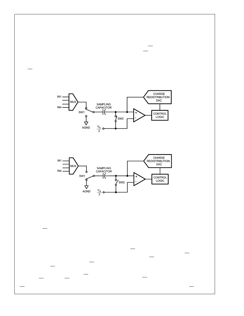
1.0 ADC124S021 OPERATION
The ADC124S021 is a successive-approximation analog-to-
digital converter designed around a charge-redistribution
digital-to-analog converter. Simplified schematics of the
ADC124S021 in both track and hold modes are shown in
Figures 1, 2
, respectively. In
Figure 1
, the ADC124S021 is in
track mode: switch SW1 connects the sampling capacitor to
one of four analog input channels through the multiplexer,
and
SW2
balances
the
ADC124S021 is in this state for the first three SCLK cycles
after CS is brought low.
Figure 2
shows the ADC124S021 in hold mode: switch SW1
connects the sampling capacitor to ground, maintaining the
comparator
inputs.
The
sampled voltage, and switch SW2 unbalances the compara-
tor. The control logic then instructs the charge-redistribution
DAC to add fixed amounts of charge to the sampling capaci-
tor until the comparator is balanced. When the comparator is
balanced, the digital word supplied to the DAC is the digital
representation
of
the
analog
ADC124S021 is in this state for the fourth through sixteenth
SCLK cycles after CS is brought low.
The time when CS is low is considered a serial frame. Each
of these frames should contain an integer multiple of 16
SCLK cycles, during which time a conversion is performed
and clocked out at the DOUT pin and data is clocked into the
DIN pin to indicate the multiplexer address for the next
conversion.
input
voltage.
The
2.0 USING THE ADC124S021
AnADC124S021 timing diagram and a serial interface timing
diagram for the ADC124S021 are shown in the Timing Dia-
grams section. CS is chip select, which initiates conversions
and frames the serial data transfers. SCLK (serial clock)
controls both the conversion process and the timing of serial
data. DOUT is the serial data output pin, where a conversion
result is sent as a serial data stream, MSB first. Data to be
written to the ADC124S021’s Control Register is placed on
DIN, the serial data input pin. New data is written to DIN with
each conversion.
A serial frame is initiated on the falling edge of CS and ends
on the rising edge of CS. Each frame must contain an integer
multiple of 16 rising SCLK edges. The ADC output data
(DOUT) is in a high impedance state when CS is high and is
active when CS is low. Thus, CS acts as an output enable.
Additionally, the device goes into a power down state when
CS is high, and also between continuous conversion cycles.
During the first 3 cycles of SCLK, the ADC is in the track
mode, acquiring the input voltage. For the next 13 SCLK
cycles the conversion is accomplished and the data is
clocked out, MSB first, starting on the 5th clock. If there is
more than one conversion in a frame, the ADC will re-enter
the track mode on the falling edge of SCLK after the N*16th
rising edge of SCLK, and re-enter the hold/convert mode on
the N*16+4th falling edge of SCLK, where "N" is an integer.
When CS is brought high, SCLK is internally gated off. If
SCLK is stopped in the low state while CS is high, the
subsequent fall of CS will generate a falling edge of the
internal version of SCLK, putting the ADC into the track
mode. This is seen by the ADC as the first falling edge of
SCLK. If SCLK is stopped with SCLK high, the ADC enters
the track mode on the first falling edge of SCLK after the
falling edge of CS.
During each conversion, data is clocked into the DIN pin on
the first 8 rising edges of SCLK after the fall of CS. For each
20124309
FIGURE 1. ADC124S021 in Track Mode
20124310
FIGURE 2. ADC124S021 in Hold Mode
A
www.national.com
15
相关PDF资料 |
PDF描述 |
|---|---|
| ADC124S021EVAL | 4 Channel, 200 kSPS, 12-Bit A/D Converter |
| ADC0854CCN | Multiplexed Comparator with 8-Bit Reference Divider |
| ADC0852 | Synchronous 4-Bit Up/Down Counters With Up/Down Mode Control 16-PDIP 0 to 70 |
| ADC0852CCN | Multiplexed Comparator with 8-Bit Reference Divider |
| ADC0858BIN | 8-Bit Analog Data Acquisition and Monitoring Systems |
相关代理商/技术参数 |
参数描述 |
|---|---|
| ADC124S021CIMMX/NOPB | 功能描述:模数转换器 - ADC RoHS:否 制造商:Texas Instruments 通道数量:2 结构:Sigma-Delta 转换速率:125 SPs to 8 KSPs 分辨率:24 bit 输入类型:Differential 信噪比:107 dB 接口类型:SPI 工作电源电压:1.7 V to 3.6 V, 2.7 V to 5.25 V 最大工作温度:+ 85 C 安装风格:SMD/SMT 封装 / 箱体:VQFN-32 |
| ADC124S021EVAL | 功能描述:模数转换器 - ADC ADC124S021EVAL BOARD RoHS:否 制造商:Texas Instruments 通道数量:2 结构:Sigma-Delta 转换速率:125 SPs to 8 KSPs 分辨率:24 bit 输入类型:Differential 信噪比:107 dB 接口类型:SPI 工作电源电压:1.7 V to 3.6 V, 2.7 V to 5.25 V 最大工作温度:+ 85 C 安装风格:SMD/SMT 封装 / 箱体:VQFN-32 |
| ADC124S051 | 制造商:NSC 制造商全称:National Semiconductor 功能描述:4 Channel, 500 kSPS, 12-Bit A/D Converter |
| ADC124S051CIMM | 功能描述:模数转换器 - ADC RoHS:否 制造商:Texas Instruments 通道数量:2 结构:Sigma-Delta 转换速率:125 SPs to 8 KSPs 分辨率:24 bit 输入类型:Differential 信噪比:107 dB 接口类型:SPI 工作电源电压:1.7 V to 3.6 V, 2.7 V to 5.25 V 最大工作温度:+ 85 C 安装风格:SMD/SMT 封装 / 箱体:VQFN-32 |
| ADC124S051CIMM/NOPB | 功能描述:模数转换器 - ADC RoHS:否 制造商:Texas Instruments 通道数量:2 结构:Sigma-Delta 转换速率:125 SPs to 8 KSPs 分辨率:24 bit 输入类型:Differential 信噪比:107 dB 接口类型:SPI 工作电源电压:1.7 V to 3.6 V, 2.7 V to 5.25 V 最大工作温度:+ 85 C 安装风格:SMD/SMT 封装 / 箱体:VQFN-32 |
发布紧急采购,3分钟左右您将得到回复。