- 您现在的位置:买卖IC网 > PDF目录2064 > ADCLK948BCPZ-REEL7 (Analog Devices Inc)IC CLOCK BUFFER MUX 2:8 32-LFCSP PDF资料下载
参数资料
| 型号: | ADCLK948BCPZ-REEL7 |
| 厂商: | Analog Devices Inc |
| 文件页数: | 1/12页 |
| 文件大小: | 0K |
| 描述: | IC CLOCK BUFFER MUX 2:8 32-LFCSP |
| 标准包装: | 1,500 |
| 系列: | SIGe |
| 类型: | 扇出缓冲器(分配),多路复用器 |
| 电路数: | 1 |
| 比率 - 输入:输出: | 2:8 |
| 差分 - 输入:输出: | 是/是 |
| 输入: | CML,CMOS,LVDS,LVPECL |
| 输出: | LVPECL |
| 频率 - 最大: | 4.8GHz |
| 电源电压: | 2.97 V ~ 3.63 V |
| 工作温度: | -40°C ~ 85°C |
| 安装类型: | 表面贴装 |
| 封装/外壳: | 32-VFQFN 裸露焊盘,CSP |
| 供应商设备封装: | 32-LFCSP-VQ |
| 包装: | 带卷 (TR) |
Two Selectable Inputs, 8 LVPECL Outputs,
SiGe Clock Fanout Buffer
ADCLK948
Rev. A
Information furnished by Analog Devices is believed to be accurate and reliable. However, no
responsibilityis assumedbyAnalogDevicesforitsuse,norforanyinfringementsof patentsorother
rightsofthirdpartiesthatmayresultfromitsuse.Specificationssubjecttochangewithoutnotice.No
license is granted by implication or otherwise under any patent or patent rights of Analog Devices.
Trademarksandregisteredtrademarksarethepropertyoftheirrespectiveowners.
One Technology Way, P.O. Box 9106, Norwood, MA 02062-9106, U.S.A.
Tel: 781.329.4700
www.analog.com
Fax: 781.461.3113
2009–2010 Analog Devices, Inc. All rights reserved.
FEATURES
2 selectable differential inputs
4.8 GHz operating frequency
75 fs rms broadband random jitter
On-chip input terminations
3.3 V power supply
APPLICATIONS
Low jitter clock distribution
Clock and data signal restoration
Level translation
Wireless communications
Wired communications
Medical and industrial imaging
ATE and high performance instrumentation
GENERAL DESCRIPTION
The ADCLK948 is an ultrafast clock fanout buffer fabricated
on the Analog Devices, Inc., proprietary XFCB3 silicon germanium
(SiGe) bipolar process. This device is designed for high speed
applications requiring low jitter.
The ADCLK948 is an ultrafast clock fanout buffer fabricated
on the Analog Devices, Inc., proprietary XFCB3 silicon germanium
(SiGe) bipolar process. This device is designed for high speed
applications requiring low jitter.
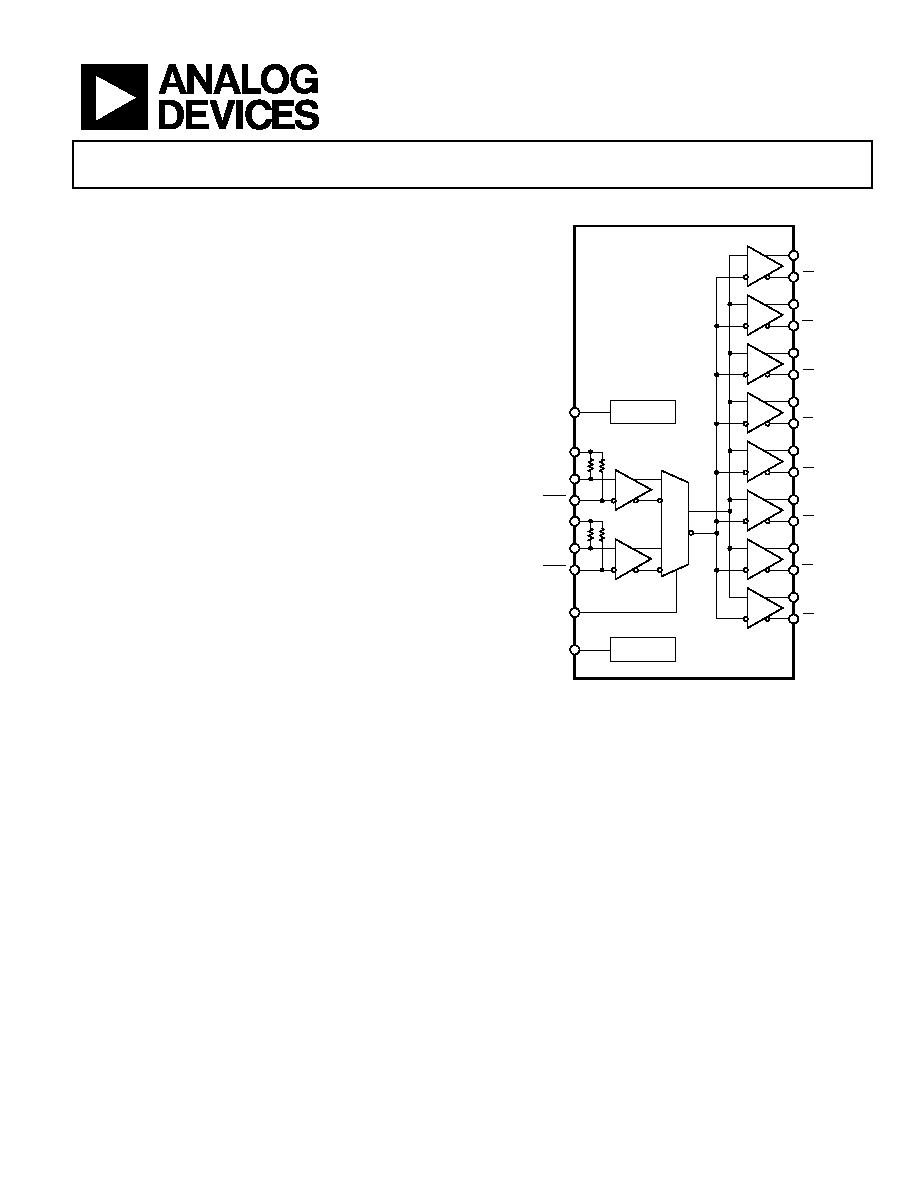
The device has two selectable differential inputs via the IN_SEL
control pin. Both inputs are equipped with center tapped,
differential, 100 Ω on-chip termination resistors. The inputs
accept dc-coupled LVPECL, CML, 3.3 V CMOS (single-ended),
and ac-coupled 1.8 V CMOS, LVDS, and LVPECL inputs. A
VREFx pin is available for biasing ac-coupled inputs.
The ADCLK948 features eight full-swing emitter coupled logic
(ECL) output drivers. For LVPECL (positive ECL) operation,
bias VCC to the positive supply and VEE to ground. For ECL
operation, bias VCC to ground and VEE to the negative supply.
The ADCLK948 features eight full-swing emitter coupled logic
(ECL) output drivers. For LVPECL (positive ECL) operation,
bias VCC to the positive supply and VEE to ground. For ECL
operation, bias VCC to ground and VEE to the negative supply.
The output stages are designed to directly drive 800 mV each
side into 50 Ω terminated to VCC 2 V for a total differential
output swing of 1.6 V.
The output stages are designed to directly drive 800 mV each
side into 50 Ω terminated to VCC 2 V for a total differential
output swing of 1.6 V.
The ADCLK948 is available in a 32-lead LFCSP and specified
for operation over the standard industrial temperature range of
40°C to +85°C.
The ADCLK948 is available in a 32-lead LFCSP and specified
for operation over the standard industrial temperature range of
40°C to +85°C.
FUNCTIONAL BLOCK DIAGRAM
Q0
Q1
Q2
Q3
Q4
Q5
Q6
Q7
VT0
VREF0
VREF1
IN_SEL
CLK0
VT1
CLK1
LVPECL
ADCLK948
REFERENCE
08
28
0-
0
01
Figure 1.
相关PDF资料 |
PDF描述 |
|---|---|
| ADCLK950BCPZ | IC CLOCK BUFFER MUX 2:10 40LFCSP |
| ADCLK954BCPZ-REEL7 | IC CLOCK BUFFER MUX 2:12 40LFCSP |
| ADCMP343YRJZ-REEL7 | IC COMPARATOR DUAL OD SOT23-8 |
| ADCMP356YKS-REEL7 | IC COMP/REF PP ACTIVE HI SC70-4 |
| ADCMP361WYRJZ-RL7 | IC COMPARATOR SINGLE OD SOT23-5 |
相关代理商/技术参数 |
参数描述 |
|---|---|
| ADCLK950 | 制造商:AD 制造商全称:Analog Devices 功能描述:Two Selectable Inputs, 10 LVPECL Outputs, SiGe Clock Fanout Buffer |
| ADCLK950/PCBZ | 功能描述:BOARD EVALUATION FOR ADCLK950 RoHS:是 类别:编程器,开发系统 >> 评估演示板和套件 系列:SIGe 标准包装:1 系列:- 主要目的:电信,线路接口单元(LIU) 嵌入式:- 已用 IC / 零件:IDT82V2081 主要属性:T1/J1/E1 LIU 次要属性:- 已供物品:板,电源,线缆,CD 其它名称:82EBV2081 |
| ADCLK950BCPZ | 功能描述:IC CLOCK BUFFER MUX 2:10 40LFCSP RoHS:是 类别:集成电路 (IC) >> 时钟/计时 - 时钟缓冲器,驱动器 系列:SIGe 标准包装:74 系列:- 类型:扇出缓冲器(分配) 电路数:1 比率 - 输入:输出:1:10 差分 - 输入:输出:是/是 输入:HCSL, LVCMOS, LVDS, LVPECL, LVTTL 输出:HCSL,LVDS 频率 - 最大:400MHz 电源电压:3 V ~ 3.6 V 工作温度:-40°C ~ 85°C 安装类型:表面贴装 封装/外壳:32-VFQFN 裸露焊盘 供应商设备封装:32-QFN(5x5) 包装:管件 |
| ADCLK950BCPZ-REEL7 | 功能描述:IC CLOCK BUFFER MUX 2:10 40LFCSP RoHS:是 类别:集成电路 (IC) >> 时钟/计时 - 时钟缓冲器,驱动器 系列:SIGe 标准包装:74 系列:- 类型:扇出缓冲器(分配) 电路数:1 比率 - 输入:输出:1:10 差分 - 输入:输出:是/是 输入:HCSL, LVCMOS, LVDS, LVPECL, LVTTL 输出:HCSL,LVDS 频率 - 最大:400MHz 电源电压:3 V ~ 3.6 V 工作温度:-40°C ~ 85°C 安装类型:表面贴装 封装/外壳:32-VFQFN 裸露焊盘 供应商设备封装:32-QFN(5x5) 包装:管件 |
| ADCLK954 | 制造商:AD 制造商全称:Analog Devices 功能描述:Two Selectable Inputs, 12 LVPECL Outputs, SiGe Clock Fanout Buffer |
发布紧急采购,3分钟左右您将得到回复。