- 您现在的位置:买卖IC网 > PDF目录10800 > ADCMP341YRJZ-REEL7 (Analog Devices Inc)IC COMPARATOR DUAL OD SOT23-8 PDF资料下载
参数资料
| 型号: | ADCMP341YRJZ-REEL7 |
| 厂商: | Analog Devices Inc |
| 文件页数: | 2/12页 |
| 文件大小: | 0K |
| 描述: | IC COMPARATOR DUAL OD SOT23-8 |
| 标准包装: | 1 |
| 类型: | 带电压基准 |
| 元件数: | 2 |
| 输出类型: | 开路漏极 |
| 电压 - 电源,单路/双路(±): | 1.7 V ~ 5.5 V |
| 电流 - 输入偏压(最小值): | 0.005µA @ 1.7V |
| 电流 - 静态(最大值): | 10µA |
| 传输延迟(最大): | 10µs |
| 工作温度: | -40°C ~ 125°C |
| 封装/外壳: | SOT-23-8 |
| 安装类型: | 表面贴装 |
| 包装: | 标准包装 |
| 产品目录页面: | 764 (CN2011-ZH PDF) |
| 其它名称: | ADCMP341YRJZ-REEL7DKR |
ADCMP341/ADCMP343
Data Sheet
Rev. A | Page 10 of 12
APPLICATION INFORMATION
The ADCMP341/ADCMP343 are dual, low power comparators
with a built-in 400 mV reference that operates from 1.7 V to 5.5 V.
The comparators are 0.275% accurate with fully programmable
hysteresis, implemented using a new technique of a three-resistor
string on the input. These open-drain outputs are capable of
sinking up to 40 mA.
COMPARATORS AND INTERNAL REFERENCE
Each of the comparators has one input available externally; the
other comparator inputs are connected internally to the 400 mV
reference. The ADCMP341 has two noninverting comparators
and the ADCMP343 has two inverting comparators.
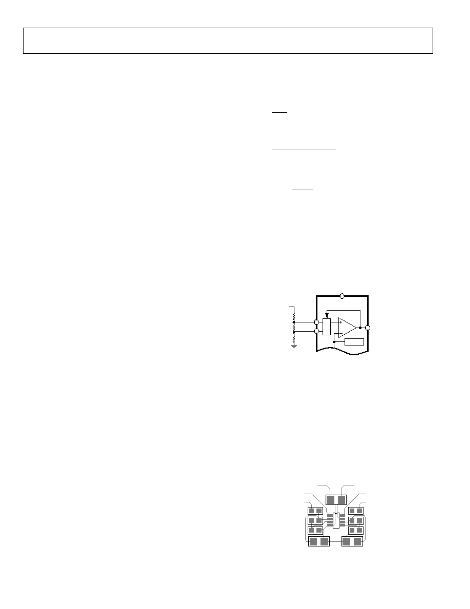
There are two input pins available to each comparator. However,
these two input pins (±INx_U, ±INx_L) connect to the same
input leg of the comparator via a muxing system. This is to
provide fully programmable rising and falling trip points. The
output of the comparator determines which pin is connected to
the input of the same comparator. Using Figure 28 as an
example, when OUTA is high, +INA_U is connected to the
comparator input. When the input voltage drops and passes
below the 400 mV reference, the output goes low. This in turn
disconnects +INA_U from the comparator and connects
+INA_L. This leg of the string is at a lower voltage and thus
instantaneously the effect of hysteresis is applied. Therefore,
using a resistor string on the input as shown in Figure 28, the
voltages for the rising and falling trip points can be programmed
by selecting the appropriate resistors in the string.
POWER SUPPLY
The ADCMP341/ADCMP343 are designed to operate from 1.7 V
to 5.5 V. A 0.1 F decoupling capacitor is recommended between
VDD and GND.
INPUTS
The comparator inputs are limited to the maximum VDD voltage
range. The voltage on these inputs can be above VDD but never
above the maximum allowed VDD voltage.
OUTPUTS
The open-drain comparator outputs are limited to the maximum
specified VDD voltage range, regardless of the VDD voltage. These
outputs are capable of sinking up to 40 mA. Outputs can be tied
together to provide a common output signal.
PROGRAMMING HYSTERESIS
When choosing the resistor values, the input bias current must
be considered as a potential source of error. Begin by choosing a
resistor value for R3, which takes into account the acceptable
error introduced by the maximum specified input bias current.
To reduce this error, the current flowing through the Resistor R3
should be considerably greater than the input bias current.
BIAS
R3
I
I >>
R3 is therefore
3
R
REF
I
V
R =
Now R2 can be calculated from the following:
(
)
FALLING
RISING
V
R
= 3
2
R1 can then be calculated using the following equation:
2
1
3
1
R
V
R
REF
RISING
×
=
where:
VREF is the specified on chip reference.
IBIAS is the maximum specified input bias current.
R1, R2, and R3 are the three resistors as shown in Figure 28.
IR3 is the current flowing through R3.
VFALLING is the desired falling trip voltage and lower of the two.
VRISING is the desired rising trip voltage and higher of the two.
+INA_U
OUTA
M
UX
VDD
400mV
ADCMP341
+INA_L
VINA
R1
R2
R3
06500-
027
Figure 28. Programming Hysteresis Example
LAYOUT RECOMMENDATIONS
Correct layout is very important to increase noise immunity.
Long tracks from the input resistors to the device can lead to
noise being coupled onto the inputs. To avoid this, it is best to
place the input resistors as close as possible to the device. It is
also recommended that a GND plane is used under this layout.
The combination of small hysteresis and the use of a large R3
resistor further increases susceptibility to noise. In this case, a
decoupling capacitor (CA, CB) may be required on the ±INx_U
node to help reduce any noise. A recommended layout example
can be seen in Figure 29.
C1
CA
CB
U1
GND
VDD
OUTA
INA
R1A
R2A
R3A
OUTB
INB
R1B
R2B
R3B
06500-
028
Figure 29. Recommended Layout Example
相关PDF资料 |
PDF描述 |
|---|---|
| AD7248JN | IC DAC 12BIT W/REF 20-DIP |
| VE-2TK-IW-S | CONVERTER MOD DC/DC 40V 100W |
| VE-J50-MY-S | CONVERTER MOD DC/DC 5V 50W |
| VE-2T2-IW-S | CONVERTER MOD DC/DC 15V 100W |
| VI-JTN-MY-S | CONVERTER MOD DC/DC 18.5V 50W |
相关代理商/技术参数 |
参数描述 |
|---|---|
| ADCMP343 | 制造商:AD 制造商全称:Analog Devices 功能描述:Dual 0.275% Comparators and Reference with Programmable Hysteresis |
| ADCMP343ARJ | 制造商:AD 制造商全称:Analog Devices 功能描述:Dual Comparators with 400mV Reference and programmable Hysteresis |
| ADCMP343YRJZ-REEL7 | 功能描述:IC COMPARATOR DUAL OD SOT23-8 RoHS:是 类别:集成电路 (IC) >> 线性 - 比较器 系列:- 标准包装:25 系列:- 类型:带电压基准 元件数:4 输出类型:CMOS,开路漏极,TTL 电压 - 电源,单路/双路(±):2 V ~ 11 V,±1 V ~ 5.5 V 电压 - 输入偏移(最小值):10mV @ 5V 电流 - 输入偏压(最小值):- 电流 - 输出(标准):0.015mA @ 5V 电流 - 静态(最大值):8.5µA CMRR, PSRR(标准):80dB CMRR,80dB PSRR 传输延迟(最大):12µs 磁滞:50mV 工作温度:0°C ~ 70°C 封装/外壳:16-DIP(0.300",7.62mm) 安装类型:通孔 包装:管件 |
| ADCMP343YRJZ-REEL7 | 制造商:Analog Devices 功能描述:IC GEN PUR COMP DUAL 8S SOT-23-8 |
| ADCMP350 | 制造商:AD 制造商全称:Analog Devices 功能描述:Comparator and Reference Circuits |
发布紧急采购,3分钟左右您将得到回复。