- 您现在的位置:买卖IC网 > PDF目录10798 > ADCMP603BCPZ-R7 (Analog Devices Inc)IC COMP TTL/CMOS 1CHAN 12-LFCSP PDF资料下载
参数资料
| 型号: | ADCMP603BCPZ-R7 |
| 厂商: | Analog Devices Inc |
| 文件页数: | 2/16页 |
| 文件大小: | 0K |
| 描述: | IC COMP TTL/CMOS 1CHAN 12-LFCSP |
| 标准包装: | 1 |
| 类型: | 带锁销 |
| 元件数: | 1 |
| 输出类型: | CMOS,补充型,满摆幅,TTL |
| 电压 - 电源,单路/双路(±): | 2.5 V ~ 5.5 V |
| 电压 - 输入偏移(最小值): | 5mV @ 2.5V |
| 电流 - 输入偏压(最小值): | 5µA @ 2.5V |
| 电流 - 输出(标准): | 50mA |
| 电流 - 静态(最大值): | 1.8mA |
| CMRR, PSRR(标准): | 50dB CMRR,50dB PSRR |
| 传输延迟(最大): | 5ns |
| 磁滞: | 100µV |
| 工作温度: | -40°C ~ 125°C |
| 封装/外壳: | 12-VFQFN 裸露焊盘,CSP |
| 安装类型: | 表面贴装 |
| 包装: | 标准包装 |
| 产品目录页面: | 765 (CN2011-ZH PDF) |
| 其它名称: | ADCMP603BCPZ-R7DKR |
ADCMP603
Rev. 0 | Page 10 of 16
APPLICATION INFORMATION
POWER/GROUND LAYOUT AND BYPASSING
This delay is measured to the 50% point for the supply in use;
therefore, the fastest times are observed with the VCC supply at
2.5 V, and larger values are observed when driving loads that
switch at other levels.
The ADCMP603 comparator is a very high speed device. Despite
the low noise output stage, it is essential to use proper high speed
design techniques to achieve the specified performance. Because
comparators are uncompensated amplifiers, feedback in any phase
relationship is likely to cause oscillations or undesired hysteresis. Of
critical importance is the use of low impedance supply planes,
particularly the output supply plane (V
When duty cycle accuracy is critical, the logic being driven
should switch at 50% of VCC and load capacitance should be
minimized. When in doubt, it is best to power VCCO or the
entire device from the logic supply and rely on the input PSRR
and CMRR to reject noise.
CCO
) and the ground plane
(GND). Individual supply planes are recommended as part of a
multilayer board. Providing the lowest inductance return path for
switching currents ensures the best possible performance in the
target application.
Overdrive and input slew rate dispersions are not significantly
affected by output loading and VCC variations.
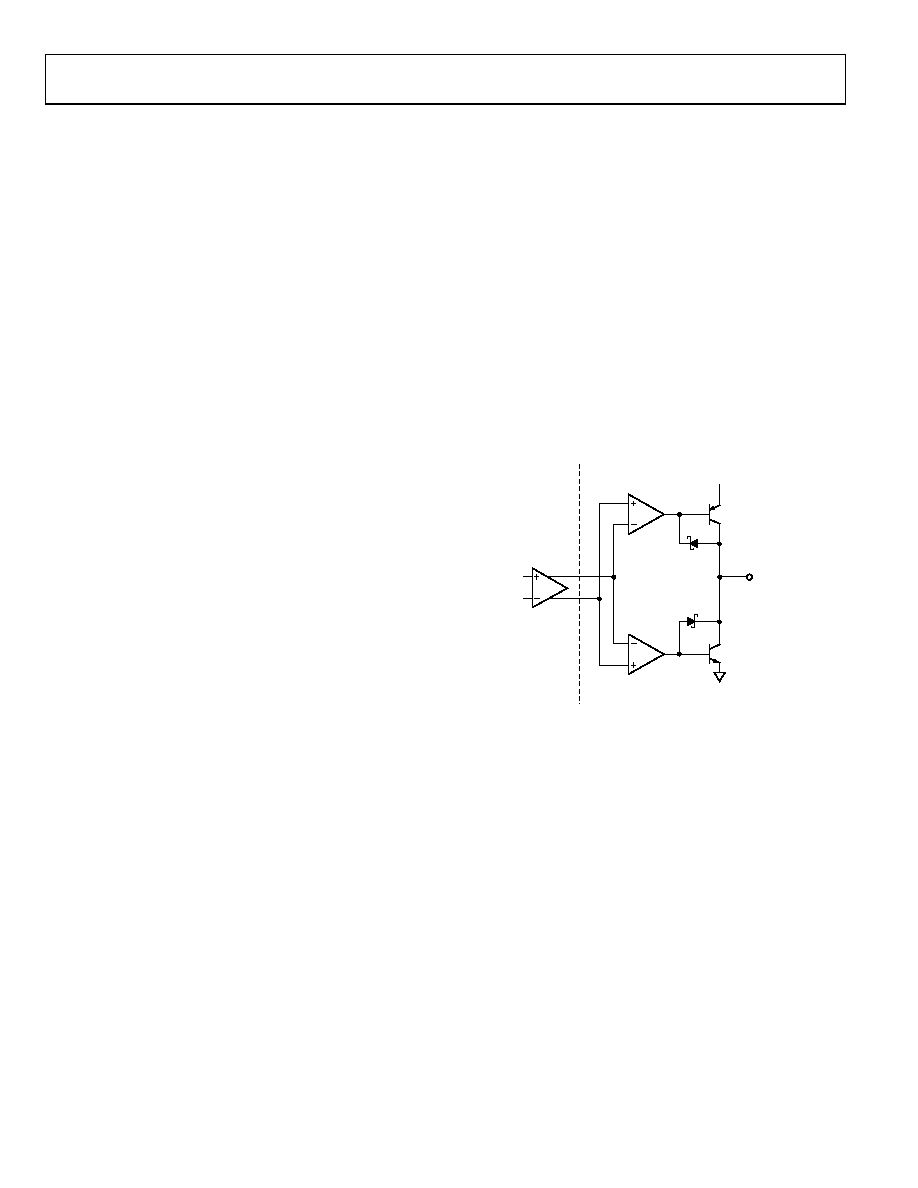
The TTL-/CMOS-compatible output stage is shown in the
simplified schematic diagram (Figure 14). Because of its
inherent symmetry and generally good behavior, this output
stage is readily adaptable for driving various filters and other
unusual loads.
It is also important to adequately bypass the input and output
supplies. Multiple high quality 0.01 μF bypass capacitors should
be placed as close as possible to each of the VCCI and VCCO supply
pins and should be connected to the GND plane with redundant
vias. At least one of these should be placed to provide a physically
short return path for output currents flowing back from ground
to the V
OUTPUT
Q2
Q1
+IN
–IN
OUTPUT STAGE
VLOGIC
GAIN STAGE
A2
A1
AV
0
59
15
-01
2
CCO
pin. High frequency bypass capacitors should be
carefully selected for minimum inductance and ESR. Parasitic
layout inductance should also be strictly controlled to maximize
the effectiveness of the bypass at high frequencies.
If the input and output supplies have been connected separately
such that VCCI ≠ VCCO, care should be taken to bypass each of
these supplies separately to the GND plane. A bypass between
them is futile and defeats the purpose of having separate pins. It
is recommended that the GND plane separate the VCCI and VCCO
planes when the circuit board layout is designed to minimize
coupling between the two supplies and to take advantage of the
additional bypass capacitance from each respective supply to
the ground plane. This enhances the performance when split
input/output supplies are used. If the input and output supplies
are connected together for single-supply operation such that V
Figure 14. Simplified Schematic Diagram of
TTL-/CMOS-Compatible Output Stage
CCI
=
V
USING/DISABLING THE LATCH FEATURE
CCO
, coupling between the two supplies is unavoidable; however,
careful board placement can help keep output return currents
away from the inputs.
The latch input is designed for maximum versatility. It can
safely be left floating for fixed hysteresis or be tied to VCC to
remove the hysteresis, or it can be driven low by any standard
TTL/CMOS device as a high speed latch.
TTL-/CMOS-COMPATIBLE OUTPUT STAGE
Specified propagation delay performance can be achieved only
by keeping the capacitive load at or below the specified minimums.
The low skew complementary outputs of the ADCMP603 are
designed to directly drive one Schottky TTL or three low power
Schottky TTL loads or the equivalent. For large fan outputs,
buses, or transmission lines, use an appropriate buffer to
maintain the excellent speed and stability of the comparator.
In addition, the pin can be operated as a hysteresis control pin
with a bias voltage of 1.25 V nominal and an input resistance of
approximately 7000 Ω, allowing the comparator hysteresis to be
easily controlled by either a resistor or an inexpensive CMOS DAC.
Hysteresis control and latch mode can be used together if an
open drain, an open collector, or a three-state driver is connected
parallel to the hysteresis control resistor or current source.
With the rated 5 pF load capacitance applied, more than half of
the total device propagation delay is output stage slew time,
even at 2.5 V V
Due to the programmable hysteresis feature, the logic threshold
of the latch pin is approximately 1.1 V regardless of VCC.
CC
. Because of this, the total prop delay decreases
as VCCO decreases, and instability in the power supply may
appear as excess delay dispersion.
相关PDF资料 |
PDF描述 |
|---|---|
| VE-B43-IV-S | CONVERTER MOD DC/DC 24V 150W |
| VE-2WX-IW-S | CONVERTER MOD DC/DC 5.2V 100W |
| VE-JNM-MW-F3 | CONVERTER MOD DC/DC 10V 100W |
| VI-J5X-MY-S | CONVERTER MOD DC/DC 5.2V 50W |
| VI-J5W-MY-S | CONVERTER MOD DC/DC 5.5V 50W |
相关代理商/技术参数 |
参数描述 |
|---|---|
| ADCMP603BCPZ-WP | 功能描述:IC COMP TTL/CMOS 1CHAN 12-LFCSP RoHS:是 类别:集成电路 (IC) >> 线性 - 比较器 系列:- 产品培训模块:Lead (SnPb) Finish for COTS Obsolescence Mitigation Program 标准包装:2,500 系列:- 类型:通用 元件数:1 输出类型:CMOS,推挽式,满摆幅,TTL 电压 - 电源,单路/双路(±):2.5 V ~ 5.5 V,±1.25 V ~ 2.75 V 电压 - 输入偏移(最小值):5mV @ 5.5V 电流 - 输入偏压(最小值):1pA @ 5.5V 电流 - 输出(标准):- 电流 - 静态(最大值):24µA CMRR, PSRR(标准):80dB CMRR,80dB PSRR 传输延迟(最大):450ns 磁滞:±3mV 工作温度:-40°C ~ 85°C 封装/外壳:6-WFBGA,CSPBGA 安装类型:表面贴装 包装:管件 其它名称:Q3554586 |
| ADCMP604 | 制造商:AD 制造商全称:Analog Devices 功能描述:Rail-to-Rail, Very Fast, 2.5 V to 5.5 V, Single-Supply LVDS Comparators |
| ADCMP604_07 | 制造商:AD 制造商全称:Analog Devices 功能描述:Rail-to-Rail, Very Fast, 2.5 V to 5.5 V, Single-Supply LVDS Comparators |
| ADCMP604BKSZ | 制造商:Analog Devices 功能描述:COMPARATOR SGL R-R I/P 5.5V 6PIN SC-70 - Bulk |
| ADCMP604BKSZ-R2 | 功能描述:IC COMP TTL/CMOS 1CHAN SC70-6 RoHS:是 类别:集成电路 (IC) >> 线性 - 比较器 系列:- 标准包装:1 系列:- 类型:通用 元件数:1 输出类型:CMOS,开路集电极,TTL 电压 - 电源,单路/双路(±):2.7 V ~ 5.5 V 电压 - 输入偏移(最小值):7mV @ 5V 电流 - 输入偏压(最小值):0.25µA @ 5V 电流 - 输出(标准):84mA @ 5V 电流 - 静态(最大值):120µA CMRR, PSRR(标准):- 传输延迟(最大):600ns 磁滞:- 工作温度:-40°C ~ 85°C 封装/外壳:SC-74A,SOT-753 安装类型:表面贴装 包装:剪切带 (CT) 产品目录页面:1268 (CN2011-ZH PDF) 其它名称:*LMV331M5*LMV331M5/NOPBLMV331M5CT |
发布紧急采购,3分钟左右您将得到回复。