- 您现在的位置:买卖IC网 > PDF目录10742 > ADCMP606BKSZ-R2 (Analog Devices Inc)IC COMP TTL/CMOS 1CHAN SC70-6 PDF资料下载
参数资料
| 型号: | ADCMP606BKSZ-R2 |
| 厂商: | Analog Devices Inc |
| 文件页数: | 3/16页 |
| 文件大小: | 0K |
| 描述: | IC COMP TTL/CMOS 1CHAN SC70-6 |
| 标准包装: | 1 |
| 类型: | 通用 |
| 元件数: | 1 |
| 输出类型: | CML,补充型,满摆幅 |
| 电压 - 电源,单路/双路(±): | 2.5 V ~ 5.5 V |
| 电压 - 输入偏移(最小值): | 5mV @ 2.5V |
| 电流 - 输入偏压(最小值): | 5µA @ 2.5V |
| 电流 - 输出(标准): | 50mA |
| 电流 - 静态(最大值): | 26mA |
| CMRR, PSRR(标准): | 50dB CMRR,50dB PSRR |
| 传输延迟(最大): | 2.1ns |
| 磁滞: | 100µV |
| 工作温度: | -40°C ~ 125°C |
| 封装/外壳: | 6-TSSOP,SC-88,SOT-363 |
| 安装类型: | 表面贴装 |
| 包装: | 标准包装 |
| 其它名称: | ADCMP606BKSZ-R2DKR |
ADCMP606/ADCMP607
Rev. A | Page 11 of 16
COMPARATOR PROPAGATION DELAY
DISPERSION
The ADCMP606/ADCMP607 comparators are designed to
reduce propagation delay dispersion over a wide input overdrive
range of 5 mV to VCCI 1 V. Propagation delay dispersion is the
variation in propagation delay that results from a change in the
degree of overdrive or slew rate (that is, how far or how fast the
input signal exceeds the switching threshold).
Propagation delay dispersion is a specification that becomes
important in high speed, time-critical applications, such as data
communication, automatic test and measurement, and instru-
mentation. It is also important in event-driven applications, such
as pulse spectroscopy, nuclear instrumentation, and medical
imaging. Dispersion is defined as the variation in propagation
delay as the input overdrive conditions are changed (Figure 15
and Figure 16).
The device dispersion is typically 2.3 ns as the overdrive varies
from 10 mV to 125 mV. This specification applies to both
positive and negative signals because each device has very closely
matched delays for positive-going and negative-going inputs as
well as very low output skews.
Q/Q OUTPUT
INPUT VOLTAGE
500mV OVERDRIVE
10mV OVERDRIVE
DISPERSION
VN ± VOS
05
91
7-
0
14
Figure 15. Propagation Delay—Overdrive Dispersion
Q/Q OUTPUT
INPUT VOLTAGE
10V/ns
1V/ns
DISPERSION
VN ± VOS
05
91
7-
0
15
Figure 16. Propagation Delay—Slew Rate Dispersion
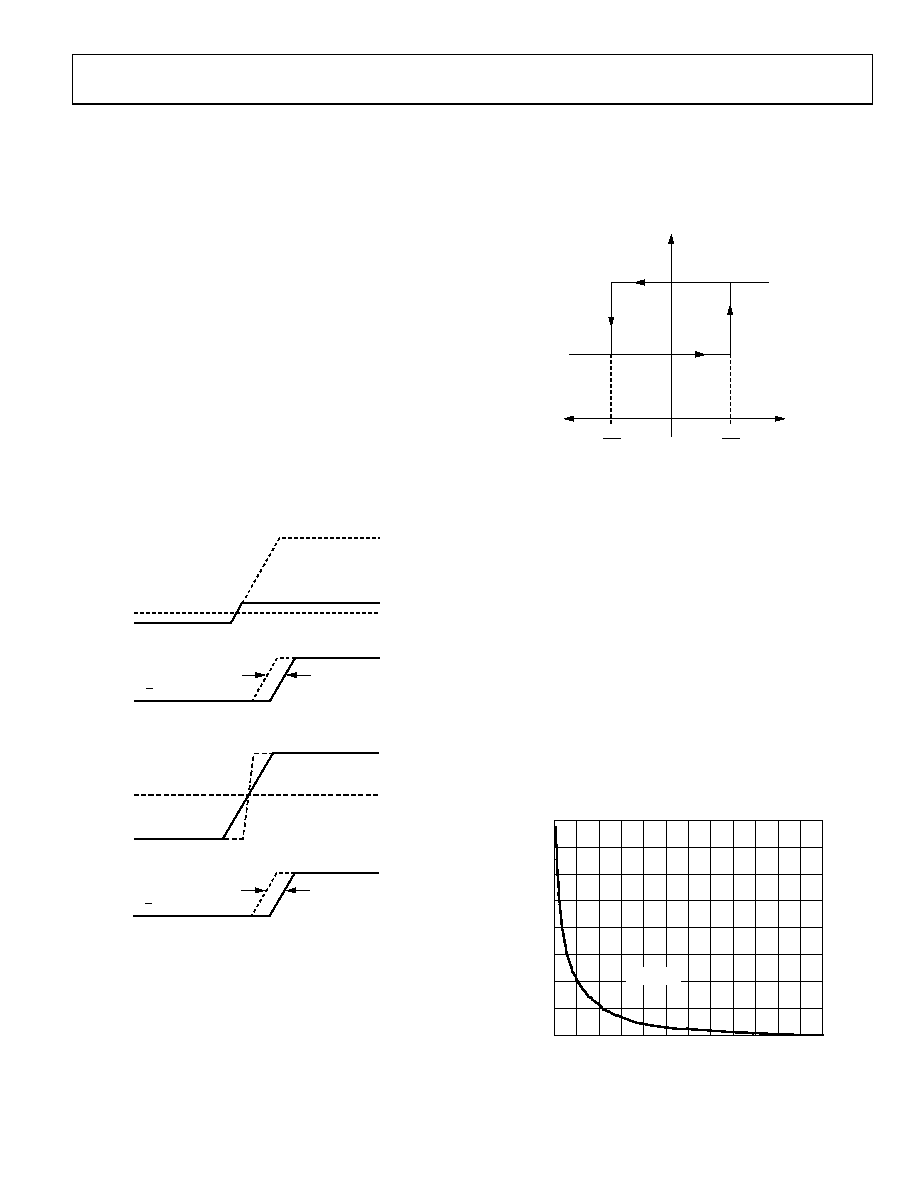
COMPARATOR HYSTERESIS
The addition of hysteresis to a comparator is often desirable in
a noisy environment, or when the differential input amplitudes
are relatively small or slow moving. Figure 17 shows the transfer
function for a comparator with hysteresis. As the input voltage
approaches the threshold (0 V, in this example) from below the
threshold region in a positive direction, the comparator switches
from low to high when the input crosses +VH/2, and the new
switching threshold becomes VH/2. The comparator remains in
the high state until the new threshold, VH/2, is crossed from
below the threshold region in a negative direction. In this manner,
noise or feedback output signals centered on 0 V input cannot
cause the comparator to switch states unless it exceeds the region
bounded by ±VH/2.
OUTPUT
INPUT
0
VOL
VOH
+VH
2
–VH
2
05
91
7-
0
16
Figure 17. Comparator Hysteresis Transfer Function
The customary technique for introducing hysteresis into a
comparator uses positive feedback from the output back to
the input. One limitation of this approach is that the amount
of hysteresis varies with the output logic levels, resulting in
hysteresis that is not symmetric about the threshold. The
external feedback network can also introduce significant
parasitics that reduce high speed performance and induce
oscillation in some cases.
This ADCMP607 comparator offers a programmable hysteresis
feature that can significantly improve accuracy and stability.
Connecting an external pull-down resistor or a current source
from the LE/HYS pin to GND, varies the amount of hysteresis
in a predictable, stable manner. Leaving the LE/HYS pin discon-
nected or driving this pin high removes hysteresis. The maximum
hysteresis that can be applied using this pin is approximately
160 mV. Figure 18 illustrates typical hysteresis applied as a
function of the external resistor value, and Figure 7 illustrates
typical hysteresis as a function of the current.
H
Y
ST
ER
ES
IS
(
m
V)
HYS RESISTOR (k)
0
50
100
150
200
250
300
350
400
50 100 150 200 250 300 350 400 450 500 550 600 650
VCC = 2.5V
05
91
7-
01
7
Figure 18. Hysteresis vs. RHYS Control Resistor
相关PDF资料 |
PDF描述 |
|---|---|
| VE-JNM-MY-F4 | CONVERTER MOD DC/DC 10V 50W |
| MAX976EUA+ | IC COMPARATOR DUAL 8-UMAX |
| ISL98003INZ-110 | IC AFE 3CH 8BIT 110MHZ 80EPTQFP |
| MAX975EUA+ | IC COMPARATOR SNGL 3V/5V 8-UMAX |
| MAX907EPA+ | IC COMPAR HS DUAL 8-DIP |
相关代理商/技术参数 |
参数描述 |
|---|---|
| ADCMP606BKSZ-REEL7 | 功能描述:IC COMP TTL/CMOS 1CHAN SC70-6 RoHS:是 类别:集成电路 (IC) >> 线性 - 比较器 系列:- 产品培训模块:Lead (SnPb) Finish for COTS Obsolescence Mitigation Program 标准包装:2,500 系列:- 类型:通用 元件数:1 输出类型:CMOS,推挽式,满摆幅,TTL 电压 - 电源,单路/双路(±):2.5 V ~ 5.5 V,±1.25 V ~ 2.75 V 电压 - 输入偏移(最小值):5mV @ 5.5V 电流 - 输入偏压(最小值):1pA @ 5.5V 电流 - 输出(标准):- 电流 - 静态(最大值):24µA CMRR, PSRR(标准):80dB CMRR,80dB PSRR 传输延迟(最大):450ns 磁滞:±3mV 工作温度:-40°C ~ 85°C 封装/外壳:6-WFBGA,CSPBGA 安装类型:表面贴装 包装:管件 其它名称:Q3554586 |
| ADCMP606BKSZ-RL | 功能描述:IC COMP TTL/CMOS 1CHAN SC70-6 RoHS:是 类别:集成电路 (IC) >> 线性 - 比较器 系列:- 产品培训模块:Lead (SnPb) Finish for COTS Obsolescence Mitigation Program 标准包装:2,500 系列:- 类型:通用 元件数:1 输出类型:CMOS,推挽式,满摆幅,TTL 电压 - 电源,单路/双路(±):2.5 V ~ 5.5 V,±1.25 V ~ 2.75 V 电压 - 输入偏移(最小值):5mV @ 5.5V 电流 - 输入偏压(最小值):1pA @ 5.5V 电流 - 输出(标准):- 电流 - 静态(最大值):24µA CMRR, PSRR(标准):80dB CMRR,80dB PSRR 传输延迟(最大):450ns 磁滞:±3mV 工作温度:-40°C ~ 85°C 封装/外壳:6-WFBGA,CSPBGA 安装类型:表面贴装 包装:管件 其它名称:Q3554586 |
| ADCMP607 | 制造商:AD 制造商全称:Analog Devices 功能描述:Rail-to-Rail, Very Fast, 2.5 V to 5.5 V, Single-Supply CML Comparators |
| ADCMP607BCPZ-R2 | 功能描述:IC COMP TTL/CMOS 1CHAN 12-LFCSP RoHS:是 类别:集成电路 (IC) >> 线性 - 比较器 系列:- 产品培训模块:Lead (SnPb) Finish for COTS Obsolescence Mitigation Program 标准包装:2,500 系列:- 类型:通用 元件数:1 输出类型:CMOS,推挽式,满摆幅,TTL 电压 - 电源,单路/双路(±):2.5 V ~ 5.5 V,±1.25 V ~ 2.75 V 电压 - 输入偏移(最小值):5mV @ 5.5V 电流 - 输入偏压(最小值):1pA @ 5.5V 电流 - 输出(标准):- 电流 - 静态(最大值):24µA CMRR, PSRR(标准):80dB CMRR,80dB PSRR 传输延迟(最大):450ns 磁滞:±3mV 工作温度:-40°C ~ 85°C 封装/外壳:6-WFBGA,CSPBGA 安装类型:表面贴装 包装:管件 其它名称:Q3554586 |
| ADCMP607BCPZ-R7 | 功能描述:IC COMP TTL/CMOS 1CHAN 12-LFCSP RoHS:是 类别:集成电路 (IC) >> 线性 - 比较器 系列:- 产品培训模块:Lead (SnPb) Finish for COTS Obsolescence Mitigation Program 标准包装:2,500 系列:- 类型:通用 元件数:1 输出类型:CMOS,推挽式,满摆幅,TTL 电压 - 电源,单路/双路(±):2.5 V ~ 5.5 V,±1.25 V ~ 2.75 V 电压 - 输入偏移(最小值):5mV @ 5.5V 电流 - 输入偏压(最小值):1pA @ 5.5V 电流 - 输出(标准):- 电流 - 静态(最大值):24µA CMRR, PSRR(标准):80dB CMRR,80dB PSRR 传输延迟(最大):450ns 磁滞:±3mV 工作温度:-40°C ~ 85°C 封装/外壳:6-WFBGA,CSPBGA 安装类型:表面贴装 包装:管件 其它名称:Q3554586 |
发布紧急采购,3分钟左右您将得到回复。