- 您现在的位置:买卖IC网 > PDF目录2064 > ADCMP607BCPZ-R2 (Analog Devices Inc)IC COMP TTL/CMOS 1CHAN 12-LFCSP PDF资料下载
参数资料
| 型号: | ADCMP607BCPZ-R2 |
| 厂商: | Analog Devices Inc |
| 文件页数: | 12/16页 |
| 文件大小: | 0K |
| 描述: | IC COMP TTL/CMOS 1CHAN 12-LFCSP |
| 标准包装: | 250 |
| 类型: | 带锁销 |
| 元件数: | 1 |
| 输出类型: | CML,补充型,满摆幅 |
| 电压 - 电源,单路/双路(±): | 2.5 V ~ 5.5 V |
| 电压 - 输入偏移(最小值): | 5mV @ 2.5V |
| 电流 - 输入偏压(最小值): | 5µA @ 2.5V |
| 电流 - 输出(标准): | 50mA |
| 电流 - 静态(最大值): | 1.5mA |
| CMRR, PSRR(标准): | 50dB CMRR,50dB PSRR |
| 传输延迟(最大): | 2.1ns |
| 磁滞: | 100µV |
| 工作温度: | -40°C ~ 125°C |
| 封装/外壳: | 12-VFQFN 裸露焊盘,CSP |
| 安装类型: | 表面贴装 |
| 包装: | 带卷 (TR) |
ADCMP606/ADCMP607
Rev. A | Page 5 of 16
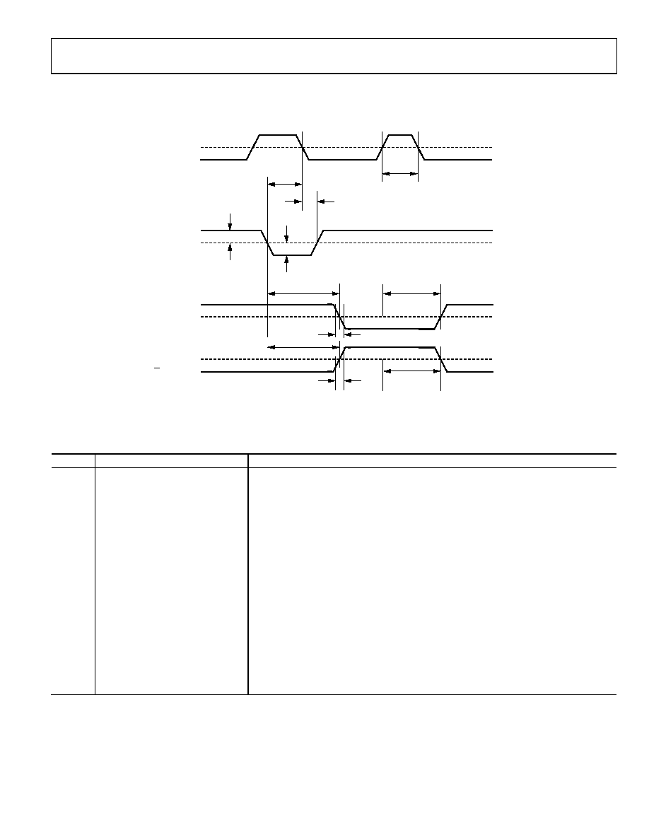
TIMING INFORMATION
Figure 2 illustrates the ADCMP606/ADCMP607 latch timing relationships. Table 2 provides definitions of the terms shown in Figure 2.
1.1V
50%
VN ± VOS
DIFFERENTIAL
INPUT VOLTAGE
LATCH ENABLE
Q OUTPUT
tH
tPDL
tPLOH
tF
VIN
VOD
tS
tPL
50%
Q OUTPUT
tPDH
tPLOL
tR
05
91
7-
0
25
Figure 2. System Timing Diagram
Table 2. Timing Descriptions
Symbol
Timing
Description
tF
Output fall time
Amount of time required to transition from a high to a low output as measured at the 20%
and 80% points.
tH
Minimum hold time
Minimum time after the negative transition of the latch enable signal that the input signal
must remain unchanged to be acquired and held at the outputs.
tPDH
Input to output high delay
Propagation delay measured from the time the input signal crosses the reference (± the
input offset voltage) to the 50% point of an output low-to-high transition.
tPDL
Input to output low delay
Propagation delay measured from the time the input signal crosses the reference (± the
input offset voltage) to the 50% point of an output high-to-low transition.
tPL
Minimum latch enable pulse width
Minimum time that the latch enable signal must be high to acquire an input signal
change.
tPLOH
Latch enable to output high delay
Propagation delay measured from the 50% point of the latch enable signal low-to-high
transition to the 50% point of an output low-to-high transition.
tPLOL
Latch enable to output low delay
Propagation delay measured from the 50% point of the latch enable signal low-to-high
transition to the 50% point of an output high-to-low transition.
tR
Output rise time
Amount of time required to transition from a low to a high output as measured at the 20%
and 80% points.
tS
Minimum setup time
Minimum time before the negative transition of the latch enable signal occurs that an
input signal change must be present to be acquired and held at the outputs.
VOD
Voltage overdrive
Difference between the input voltages VA and VB.
相关PDF资料 |
PDF描述 |
|---|---|
| ADCMP608BKSZ-R2 | IC COMP TTL/CMOS R-R SGL SC70-6 |
| ADCMP609BRMZ-REEL | IC COMP TTL/CMOS R-R SGL 8-MSOP |
| ADCMP670-1YUJZ-RL7 | IC COMPARATOR DUAL OD TSOT-23-6 |
| ADCMP671-1YUJZ-RL7 | IC MONITOR UV/OV LP ADJ 6TSOT |
| ADD8506WRUZ-REEL | IC GAMMA BUFFER LCD 6CH 24TSSOP |
相关代理商/技术参数 |
参数描述 |
|---|---|
| ADCMP607BCPZ-R7 | 功能描述:IC COMP TTL/CMOS 1CHAN 12-LFCSP RoHS:是 类别:集成电路 (IC) >> 线性 - 比较器 系列:- 产品培训模块:Lead (SnPb) Finish for COTS Obsolescence Mitigation Program 标准包装:2,500 系列:- 类型:通用 元件数:1 输出类型:CMOS,推挽式,满摆幅,TTL 电压 - 电源,单路/双路(±):2.5 V ~ 5.5 V,±1.25 V ~ 2.75 V 电压 - 输入偏移(最小值):5mV @ 5.5V 电流 - 输入偏压(最小值):1pA @ 5.5V 电流 - 输出(标准):- 电流 - 静态(最大值):24µA CMRR, PSRR(标准):80dB CMRR,80dB PSRR 传输延迟(最大):450ns 磁滞:±3mV 工作温度:-40°C ~ 85°C 封装/外壳:6-WFBGA,CSPBGA 安装类型:表面贴装 包装:管件 其它名称:Q3554586 |
| ADCMP607BCPZ-WP | 功能描述:IC COMP TTL/CMOS 1CHAN 12-LFCSP RoHS:是 类别:集成电路 (IC) >> 线性 - 比较器 系列:- 产品培训模块:Lead (SnPb) Finish for COTS Obsolescence Mitigation Program 标准包装:50 系列:- 类型:带电压基准 元件数:4 输出类型:开路漏极 电压 - 电源,单路/双路(±):2.5 V ~ 11 V,±1.25 V ~ 5.5 V 电压 - 输入偏移(最小值):10mV @ 5V 电流 - 输入偏压(最小值):- 电流 - 输出(标准):0.015mA @ 5V 电流 - 静态(最大值):8.5µA CMRR, PSRR(标准):80dB CMRR,80dB PSRR 传输延迟(最大):- 磁滞:- 工作温度:0°C ~ 70°C 封装/外壳:16-SOIC(0.154",3.90mm 宽) 安装类型:表面贴装 包装:管件 产品目录页面:1386 (CN2011-ZH PDF) |
| ADCMP608 | 制造商:AD 制造商全称:Analog Devices 功能描述:Rail-to-Rail, Fast, Low Power 2.5 V to 5.5 V, Single-Supply TTL/CMOS Comparator |
| ADCMP608_07 | 制造商:AD 制造商全称:Analog Devices 功能描述:Rail-to-Rail, Fast, Low Power 2.5 V to 5.5 V, Single-Supply TTL/CMOS Comparator |
| ADCMP608BKSZ-R2 | 功能描述:IC COMP TTL/CMOS R-R SGL SC70-6 RoHS:是 类别:集成电路 (IC) >> 线性 - 比较器 系列:- 标准包装:25 系列:- 类型:带电压基准 元件数:4 输出类型:CMOS,开路漏极,TTL 电压 - 电源,单路/双路(±):2 V ~ 11 V,±1 V ~ 5.5 V 电压 - 输入偏移(最小值):10mV @ 5V 电流 - 输入偏压(最小值):- 电流 - 输出(标准):0.015mA @ 5V 电流 - 静态(最大值):8.5µA CMRR, PSRR(标准):80dB CMRR,80dB PSRR 传输延迟(最大):12µs 磁滞:50mV 工作温度:0°C ~ 70°C 封装/外壳:16-DIP(0.300",7.62mm) 安装类型:通孔 包装:管件 |
发布紧急采购,3分钟左右您将得到回复。