- 您现在的位置:买卖IC网 > PDF目录10700 > ADCMP609BRMZ (Analog Devices Inc)IC COMP TTL/CMOS R-R SGL 8-MSOP PDF资料下载
参数资料
| 型号: | ADCMP609BRMZ |
| 厂商: | Analog Devices Inc |
| 文件页数: | 10/12页 |
| 文件大小: | 0K |
| 描述: | IC COMP TTL/CMOS R-R SGL 8-MSOP |
| 标准包装: | 50 |
| 类型: | 通用 |
| 元件数: | 1 |
| 输出类型: | CMOS,满摆幅,TTL |
| 电压 - 电源,单路/双路(±): | 2.5 V ~ 5.5 V |
| 电压 - 输入偏移(最小值): | 3mV @ 2.5V |
| 电流 - 输入偏压(最小值): | 0.4µA @ 2.5V |
| 电流 - 输出(标准): | 50mA |
| 电流 - 静态(最大值): | 1.1mA |
| CMRR, PSRR(标准): | 50dB CMRR,50dB PSRR |
| 传输延迟(最大): | 60ns |
| 磁滞: | 100µV |
| 工作温度: | -40°C ~ 125°C |
| 封装/外壳: | 8-TSSOP,8-MSOP(0.118",3.00mm 宽) |
| 安装类型: | 表面贴装 |
| 包装: | 管件 |
ADCMP608
Rev. 0 | Page 7 of 12
APPLICATION INFORMATION
OUTPUT
Q2
Q1
+IN
–IN
OUTPUT STAGE
VLOGIC
GAIN STAGE
A2
A1
AV
067
69
-00
9
POWER/GROUND LAYOUT AND BYPASSING
The ADCMP608 comparator is a high speed device. Despite the
low noise output stage, it is essential to use proper high speed
design techniques to achieve the specified performance. Because
comparators are uncompensated amplifiers, feedback in any phase
relationship is likely to cause oscillations or undesired hysteresis. Of
critical importance is the use of low impedance supply planes,
particularly the output supply plane (VCC) and the ground plane
(GND). Individual supply planes are recommended as part of a
multilayer board. Providing the lowest inductance return path for
switching currents ensures the best possible performance in the
target application.
It is also important to adequately bypass the input and output
supplies. A 0.1 μF bypass capacitor should be placed as close as
possible to the VCC supply pin. The capacitor should be connected
to the GND plane with redundant vias placed to provide a
physically short return path for output currents flowing back
from ground to the VCC pin. High frequency bypass capacitors
should be carefully selected for minimum inductance and ESR.
Parasitic layout inductance should also be strictly controlled to
maximize the effectiveness of the bypass at high frequencies.
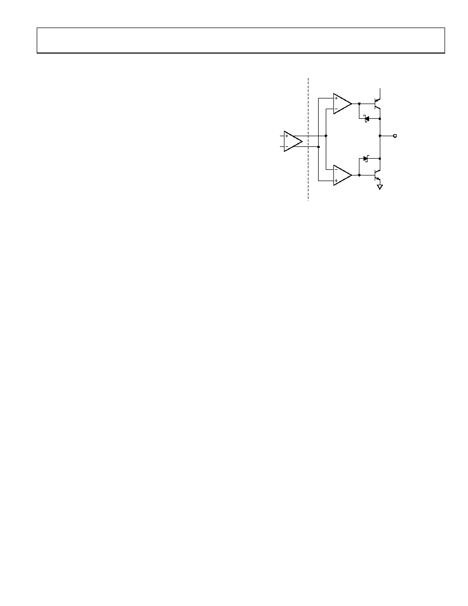
Figure 9. Simplified Schematic Diagram of
TTL-/CMOS-Compatible Output Stage
OPTIMIZING PERFORMANCE
As with any high speed comparator, proper design and layout
techniques are essential for obtaining the specified performance.
Stray capacitance, inductance, common power and ground
impedances, or other layout issues can severely limit performance
and can often cause oscillation. The source impedance should be
minimized as much as is practicable. High source impedance, in
combination with the parasitic input capacitance of the comparator,
causes an undesirable degradation in bandwidth at the input, thus
degrading the overall response. Higher impedances encourage
undesired coupling.
TTL-/CMOS-COMPATIBLE OUTPUT STAGE
Specified propagation delay performance can be achieved only
by keeping the capacitive load at or below the specified minimums.
The output of the ADCMP608 is designed to directly drive one
Schottky TTL, or three low power Schottky TTL loads, or the
equivalent. For large fan outs, buses, or transmission lines, use
an appropriate buffer to maintain the excellent speed and
stability of the comparator.
COMPARATOR PROPAGATION
DELAY DISPERSION
The ADCMP608 comparator is designed to reduce propagation
delay dispersion over a wide input overdrive range of 10 mV to
VCC – 1 V. Propagation delay dispersion is the variation in
propagation delay that results from a change in the degree of
overdrive or slew rate (how far or how fast the input signal
exceeds the switching threshold).
With the rated 15 pF load capacitance applied, more than half
of the total device propagation delay is output stage slew time.
Because of this, the total propagation delay decreases as VCC
decreases, and instability in the power supply may appear as
excess delay dispersion.
Propagation delay dispersion is a specification that becomes
important in high speed, time-critical applications, such as data
communication, automatic test and measurement, and instru-
mentation. It is also important in event-driven applications, such
as pulse spectroscopy, nuclear instrumentation, and medical
imaging. Dispersion is defined as the variation in propagation
delay as the input overdrive conditions are changed (
Delay is measured to the 50% point for whatever supply is in
use; thus, the fastest times are observed with the VCC supply at
2.5 V, and larger values are observed when driving loads that
switch at other levels.
Overdrive and input slew rate dispersions are not significantly
affected by output loading and VCC variations.
and Figure 11).
The TTL-/CMOS-compatible output stage is shown in the
simplified schematic diagram (see
ADCMP608 dispersion is typically < 12 ns as the overdrive
varies from 10 mV to 125 mV. This specification applies to
both positive and negative signals because the device has very
closely matched delays for both positive-going and negative-
going inputs, and very low output skews. Remember to add the
actual device offset to the overdrive for repeatable dispersion
measurements.
Figure 9). Because of its
inherent symmetry and generally good behavior, this output
stage is readily adaptable for driving various filters and other
unusual loads.
相关PDF资料 |
PDF描述 |
|---|---|
| B37984M5105K058 | CAP CER 1UF 50V X7R 10% RADIAL |
| LTC1440CS8#TRPBF | IC COMP W/REF LP SINGLE 8-SOIC |
| VE-JWY-MY-F1 | CONVERTER MOD DC/DC 3.3V 33W |
| LTC1440CS8#TR | IC COMP SGL LP 1.182V REF 8SOIC |
| B37984M5105K037 | CAP CER 1UF 50V X7R 10% RADIAL |
相关代理商/技术参数 |
参数描述 |
|---|---|
| ADCMP609BRMZ1 | 制造商:AD 制造商全称:Analog Devices 功能描述:Rail-to-Rail, Fast, Low Power 2.5 V to 5.5 V, Single-Supply TTL/CMOS Comparator |
| ADCMP609BRMZ-REEL | 功能描述:IC COMP TTL/CMOS R-R SGL 8-MSOP RoHS:是 类别:集成电路 (IC) >> 线性 - 比较器 系列:- 标准包装:25 系列:- 类型:带电压基准 元件数:4 输出类型:CMOS,开路漏极,TTL 电压 - 电源,单路/双路(±):2 V ~ 11 V,±1 V ~ 5.5 V 电压 - 输入偏移(最小值):10mV @ 5V 电流 - 输入偏压(最小值):- 电流 - 输出(标准):0.015mA @ 5V 电流 - 静态(最大值):8.5µA CMRR, PSRR(标准):80dB CMRR,80dB PSRR 传输延迟(最大):12µs 磁滞:50mV 工作温度:0°C ~ 70°C 封装/外壳:16-DIP(0.300",7.62mm) 安装类型:通孔 包装:管件 |
| ADCMP609BRMZ-REEL1 | 制造商:AD 制造商全称:Analog Devices 功能描述:Rail-to-Rail, Fast, Low Power 2.5 V to 5.5 V, Single-Supply TTL/CMOS Comparator |
| ADCMP609BRMZ-REEL7 | 功能描述:IC COMPARATOR TTL/CMOS 8-MSOP RoHS:是 类别:集成电路 (IC) >> 线性 - 比较器 系列:- 产品培训模块:Lead (SnPb) Finish for COTS Obsolescence Mitigation Program 标准包装:50 系列:- 类型:带电压基准 元件数:4 输出类型:开路漏极 电压 - 电源,单路/双路(±):2.5 V ~ 11 V,±1.25 V ~ 5.5 V 电压 - 输入偏移(最小值):10mV @ 5V 电流 - 输入偏压(最小值):- 电流 - 输出(标准):0.015mA @ 5V 电流 - 静态(最大值):8.5µA CMRR, PSRR(标准):80dB CMRR,80dB PSRR 传输延迟(最大):- 磁滞:- 工作温度:0°C ~ 70°C 封装/外壳:16-SOIC(0.154",3.90mm 宽) 安装类型:表面贴装 包装:管件 产品目录页面:1386 (CN2011-ZH PDF) |
| ADCMP609BRMZ-REEL71 | 制造商:AD 制造商全称:Analog Devices 功能描述:Rail-to-Rail, Fast, Low Power 2.5 V to 5.5 V, Single-Supply TTL/CMOS Comparator |
发布紧急采购,3分钟左右您将得到回复。