参数资料
| 型号: | ADDAC80D-CBI-V |
| 厂商: | Analog Devices Inc |
| 文件页数: | 3/16页 |
| 文件大小: | 0K |
| 描述: | IC DAC 12BIT LOW COST 24-CDIP |
| 产品培训模块: | Data Converter Fundamentals DAC Architectures |
| 标准包装: | 15 |
| 设置时间: | 2µs |
| 位数: | 12 |
| 数据接口: | 并联 |
| 转换器数目: | 1 |
| 电压电源: | 双 ± |
| 功率耗散(最大): | 300mW |
| 工作温度: | 0°C ~ 70°C |
| 安装类型: | 通孔 |
| 封装/外壳: | 24-CDIP(0.600",15.24mm) |
| 供应商设备封装: | 24-CDIP 侧面镀铜 |
| 包装: | 管件 |
| 输出数目和类型: | 1 电压,单极;1 电压,双极 |
| 采样率(每秒): | * |
REV. B
ADDAC80/ADDAC85/ADDAC87
–11–
VOLTAGE OUTPUT MODELS
Internal scaling resistors provided in the ADDAC80 may be
connected to produce bipolar output voltage ranges of
±10 V,
±5 V or ±2.5 V or unipolar output voltage ranges of 0 V to +5 V
or 0 V to +10 V (see Figure 9).
REF
INPUT
TO REF
CONTROL
CIRCUIT
FROM
WEIGHTED
RESISTOR
NETWORK
SUMMING
JUNCTION
6.3k
5k
18
20
16
+
–
OUTPUT
COM
BIPOLAR
OFFSET
21
15
19
17
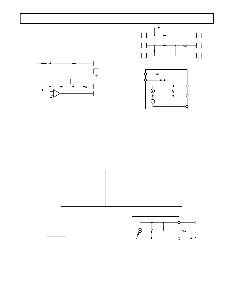
Figure 9. Output Amplifier Voltage Range Scaling Circuit
Gain and offset drift are minimized in the ADDAC80 because
of the thermal tracking of the scaling resistors with other device
components. Connections for various output voltage ranges are
shown in Table III. Settling time is specified for a full-scale
range change: 4 s for a 10 k
feedback resistor; 3 s for a 5 k
feedback resistor when using the compensation capacitor shown
in Figure 3a.
The equivalent resistive scaling network and output circuit of
the current model are shown in Figures 10 and 11. External RLS
resistors are required to produce exactly 0 V to –2 V or
± 1 V
output. TCR of these resistors should be
±100 ppm/°C or less
to maintain the ADDAC80 output specifications. If exact output
ranges are not required, the external resistors are not needed.
17
TO REF CONTROL CIRCUIT
6.3k
3k
2k
19
20
16
18
REF IN
5k
15
Figure 10. Internal Scaling Resistors
6.3k
BIPOLAR OFFSET
REFERENCE
INPUT
IOUT
COMMON
REFERENCE OUT
6.6k
V
TO REF
CONTROL
CIRCUIT
17
16
I
0 TO 2mA
6.3V
24
21
15
+
–
Figure 11. ADDAC80 Current Model Equivalent Output Circuit
Internal resistors are provided to scale an external op amp or to
configure a resistive load to offer two output voltage ranges of
±1 V
or 0 V to –2 V. These resistors (RLI TCR = 20 ppm/
°C) are an
integral part of the ADDAC80 and maintain gain and bipolar
offset drift specifications. If the internal resistors are not used, exter-
nal RL (or RF) resistors should have a TCR of
±25 ppm/°C or
less to minimize drift. This will typically add
±50 ppm/°C + the
TCR of RL (or RF) to the total drift.
Table III. Output Voltage Range Connections, Voltage Model ADDAC80
Output
Digital
Connect
Range
Input Codes
Pin 15 to
Pin 17 to
Pin 19 to
Pin 16 to
±10 V
COB or CTC
19
20
15
24
±5 V
COB or CTC
18
20
NC
24
±2.5 V
COB or CTC
18
20
24
0 V to 10 V
CSB
18
21
NC
24
0 V to 5 V
CSB
18
21
20
24
0 V to 10 V
CCD
19
NC
15
24
NC = No Connect
DRIVING A RESISTIVE LOAD UNIPOLAR
A load resistance, RL = RLI, + RLS, connected as shown in
Figure 12 will generate a voltage range, VOUT, determined by:
VmA
kR
OUT
L
=
×
+
–
.
2
66
(1)
where RL max = 1.54 k
and V
OUT max = –2.5 V
To achieve specified drift, connect the internal scaling resistor
(RLI) as shown in Table IV to an external metal film trim resistor
(RLS) to provide full scale output voltage range of 0 V to –2 V.
With RLS = 0 V, VOUT = –1.69 V.
0 TO
2mA
CURRENT CONTROLLED
BY DIGITAL INPUT
6.6k
RLI
968
COMMON
VOUT
RLS
+
–
15
18
21
Figure 12. Equivalent Circuit ADDAC80-CBI-I Connected
for Unipolar Voltage Output with Resistive Load
相关PDF资料 |
PDF描述 |
|---|---|
| AD7247KNZ | IC DAC 12BIT W/AMP W/BUFF 24-DIP |
| VI-2NW-IV-F1 | CONVERTER MOD DC/DC 5.5V 150W |
| AD7237KN | IC DAC 12BIT LC2MOS DUAL 24-DIP |
| AD5363BCPZ | IC DAC 14BIT 8CH SERIAL 56-LFCSP |
| LTC1596AISW#TRPBF | IC D/A CONV 16BIT MLTPLYNG16SOIC |
相关代理商/技术参数 |
参数描述 |
|---|---|
| ADDAC80D-CBI-V/+ | 制造商:Rochester Electronics LLC 功能描述:- Bulk |
| ADDAC80N-CBI-V | 功能描述:IC DAC 12-BIT BINARY MONO 24-DIP RoHS:否 类别:集成电路 (IC) >> 数据采集 - 数模转换器 系列:- 产品培训模块:Data Converter Fundamentals DAC Architectures 标准包装:750 系列:- 设置时间:7µs 位数:16 数据接口:并联 转换器数目:1 电压电源:双 ± 功率耗散(最大):100mW 工作温度:0°C ~ 70°C 安装类型:表面贴装 封装/外壳:28-LCC(J 形引线) 供应商设备封装:28-PLCC(11.51x11.51) 包装:带卷 (TR) 输出数目和类型:1 电压,单极;1 电压,双极 采样率(每秒):143k |
| ADDAC80N-CBI-V | 制造商:Analog Devices 功能描述:SEMICONDUCTORSL |
| ADDAC80N-CBI-V/+ | 制造商:Rochester Electronics LLC 功能描述: 制造商:Analog Devices 功能描述: |
| ADDAC80NZ-CBI-V | 功能描述:IC DAC 12-BIT BINARY MONO 24-DIP RoHS:是 类别:集成电路 (IC) >> 数据采集 - 数模转换器 系列:- 标准包装:1 系列:- 设置时间:4.5µs 位数:12 数据接口:串行,SPI? 转换器数目:1 电压电源:单电源 功率耗散(最大):- 工作温度:-40°C ~ 125°C 安装类型:表面贴装 封装/外壳:8-SOIC(0.154",3.90mm 宽) 供应商设备封装:8-SOICN 包装:剪切带 (CT) 输出数目和类型:1 电压,单极;1 电压,双极 采样率(每秒):* 其它名称:MCP4921T-E/SNCTMCP4921T-E/SNRCTMCP4921T-E/SNRCT-ND |
发布紧急采购,3分钟左右您将得到回复。