- 您现在的位置:买卖IC网 > PDF目录9103 > ADF4107BCPZ-REEL7 (Analog Devices Inc)IC PLL FREQ SYNTHESIZER 20LFCSP PDF资料下载
参数资料
| 型号: | ADF4107BCPZ-REEL7 |
| 厂商: | Analog Devices Inc |
| 文件页数: | 17/20页 |
| 文件大小: | 0K |
| 描述: | IC PLL FREQ SYNTHESIZER 20LFCSP |
| 标准包装: | 1,500 |
| 类型: | 时钟/频率合成器,RF |
| PLL: | 是 |
| 输入: | CMOS,TTL |
| 输出: | 时钟 |
| 电路数: | 1 |
| 比率 - 输入:输出: | 2:1 |
| 差分 - 输入:输出: | 是/无 |
| 频率 - 最大: | 7GHz |
| 除法器/乘法器: | 无/无 |
| 电源电压: | 2.7 V ~ 3.3 V |
| 工作温度: | -40°C ~ 85°C |
| 安装类型: | 表面贴装 |
| 封装/外壳: | 20-VFQFN 裸露焊盘,CSP |
| 供应商设备封装: | 20-LFCSP-VQ |
| 包装: | 带卷 (TR) |
ADF4107
Data Sheet
Rev. D | Page 6 of 20
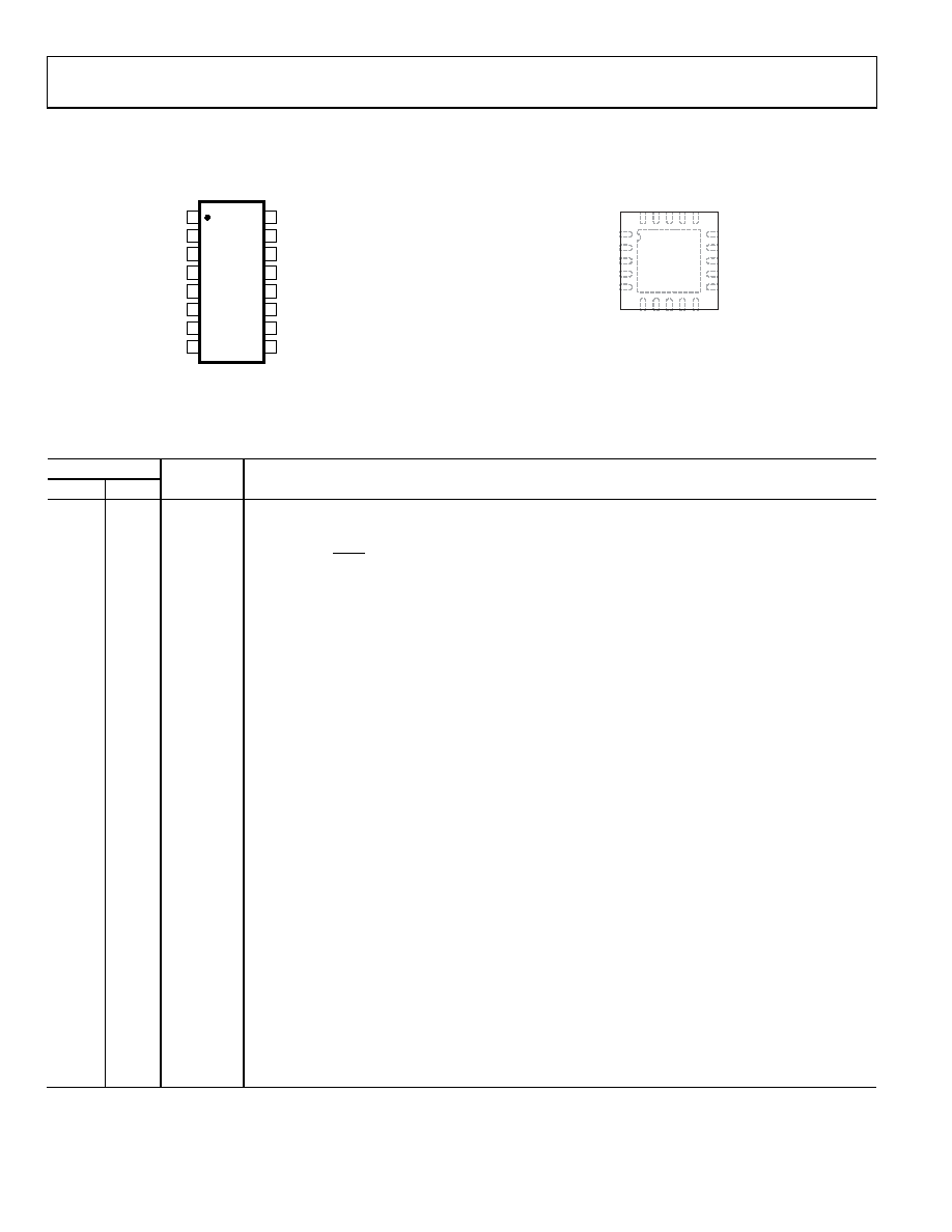
PIN CONFIGURATIONS AND FUNCTION DESCRIPTIONS
03338-
003
RSET
CP
CPGND
AGND
1
2
3
4
5
6
7
8
RFINB
RFINA
AVDD
REFIN
MUXOUT
LE
DATA
CLK
CE
DGND
16
15
14
13
12
11
10
9
VP
DVDD
TOP VIEW
(Not to Scale)
ADF4107
NOTES:
1. TRANSISTOR COUNT 6425 (CMOS),
303 (BIPOLAR).
Figure 3. Pin Configuration, TSSOP
03338-
004
14
13
12
1
3
4
LE
15 MUXOUT
DATA
CLK
11 CE
CPGND
AGND
2
AGND
RFINB
5
RFINA
7
AV
DD
6
AV
DD
8
RE
F
IN
9
DG
ND
10
DG
ND
19
R
SET
20
CP
18
V
P
17
DV
DD
16
DV
DD
ADF4107
TOP VIEW
(Not to Scale)
NOTES
1. TRANSISTOR COUNT 6425 (CMOS),
303 (BIPOLAR).
2. THE EXPOSED PAD MUST BE
CONNECTED TO AGND.
Figure 4. Pin Configuration, LFCSP
Table 4. Pin Function Descriptions
Pin No.
TSSOP
LFCSP
Mnemonic
Description
1
19
RSET
Connecting a resistor between this pin and CPGND sets the maximum charge pump output current. The
nominal voltage potential at the RSET pin is 0.66 V. The relationship between ICP and RSET is
SET
MAX
CP
R
I
5
.
25
=
so, with RSET = 5.1 k, ICPMAX = 5 mA.
2
20
CP
Charge Pump Output. When enabled, this pin provides ±ICP to the external loop filter, which in turn drives
the external VCO.
3
1
CPGND
Charge Pump Ground. This is the ground return path for the charge pump.
4
2, 3
AGND
Analog Ground. This is the ground return path of the prescaler.
5
4
RFINB
Complementary Input to the RF Prescaler. This point must be decoupled to the ground plane with a small
bypass capacitor, typically 100 pF. See Figure 18.
6
5
RFINA
Input to the RF Prescaler. This small signal input is ac-coupled to the external VCO.
7
6, 7
AVDD
Analog Power Supply. This voltage may range from 2.7 V to 3.3 V. Decoupling capacitors to the analog
ground plane should be placed as close as possible to this pin. AVDD must be the same value as DVDD.
8
REFIN
Reference Input. This is a CMOS input with a nominal threshold of VDD/2 and a dc equivalent input
resistance of 100 k. See Figure 17. This input can be driven from a TTL or CMOS crystal oscillator or it can
be ac-coupled.
9
9, 10
DGND
Digital Ground.
10
11
CE
Chip Enable. A logic low on this pin powers down the device and puts the charge pump output into three-
state mode. Taking the pin high powers up the device, depending on the status of the power-down bit, F2.
11
12
CLK
Serial Clock Input. This serial clock is used to clock in the serial data to the registers. The data is latched
into the 24-bit shift register on the CLK rising edge. This input is a high impedance CMOS input.
12
13
DATA
Serial Data Input. The serial data is loaded MSB first with the two LSBs being the control bits. This input is a
high impedance CMOS input.
13
14
LE
Load Enable, CMOS Input. When LE goes high, the data stored in the shift registers is loaded into one of
the four latches, the latch being selected using the control bits.
14
15
MUXOUT
This multiplexer output allows either the lock detect, the scaled RF, or the scaled reference frequency to
be accessed externally.
15
16, 17
DVDD
Digital Power Supply. This may range from 2.7 V to 3.3 V. Decoupling capacitors to the digital ground
plane should be placed as close as possible to this pin. DVDD must be the same value as AVDD.
16
18
VP
Charge Pump Power Supply. This voltage should be greater than or equal to VDD. In systems where VDD is 3 V, it
can be set to 5 V and used to drive a VCO with a tuning range of up to 5 V.
EP
Exposed Pad. The exposed pad must be connected to AGND.
相关PDF资料 |
PDF描述 |
|---|---|
| SY100E256JZ | IC MUX/LATCH 3BIT 4:1 28-PLCC |
| MS3450L28-11PY | CONN RCPT 22POS WALL MNT W/PINS |
| X9317UPI-2.7 | IC XDCP 100TAP 50K 3-WIRE 8-DIP |
| X9317UPI | IC XDCP 100TAP 50K 3-WIRE 8-DIP |
| MS3450L28-11PX | CONN RCPT 22POS WALL MNT W/PINS |
相关代理商/技术参数 |
参数描述 |
|---|---|
| ADF4107BRU | 功能描述:IC PLL FREQ SYNTHESIZER 16TSSOP RoHS:否 类别:集成电路 (IC) >> 时钟/计时 - 时钟发生器,PLL,频率合成器 系列:- 标准包装:1,000 系列:Precision Edge® 类型:时钟/频率合成器 PLL:无 输入:CML,PECL 输出:CML 电路数:1 比率 - 输入:输出:2:1 差分 - 输入:输出:是/是 频率 - 最大:10.7GHz 除法器/乘法器:无/无 电源电压:2.375 V ~ 3.6 V 工作温度:-40°C ~ 85°C 安装类型:表面贴装 封装/外壳:16-VFQFN 裸露焊盘,16-MLF? 供应商设备封装:16-MLF?(3x3) 包装:带卷 (TR) 其它名称:SY58052UMGTRSY58052UMGTR-ND |
| ADF4107BRU-REEL | 功能描述:IC PLL FREQ SYNTHESIZER 16-TSSOP RoHS:否 类别:集成电路 (IC) >> 时钟/计时 - 时钟发生器,PLL,频率合成器 系列:- 标准包装:1,000 系列:Precision Edge® 类型:时钟/频率合成器 PLL:无 输入:CML,PECL 输出:CML 电路数:1 比率 - 输入:输出:2:1 差分 - 输入:输出:是/是 频率 - 最大:10.7GHz 除法器/乘法器:无/无 电源电压:2.375 V ~ 3.6 V 工作温度:-40°C ~ 85°C 安装类型:表面贴装 封装/外壳:16-VFQFN 裸露焊盘,16-MLF? 供应商设备封装:16-MLF?(3x3) 包装:带卷 (TR) 其它名称:SY58052UMGTRSY58052UMGTR-ND |
| ADF4107BRU-REEL7 | 功能描述:IC PLL FREQ SYNTHESIZER 16-TSSOP RoHS:否 类别:集成电路 (IC) >> 时钟/计时 - 时钟发生器,PLL,频率合成器 系列:- 标准包装:1,000 系列:Precision Edge® 类型:时钟/频率合成器 PLL:无 输入:CML,PECL 输出:CML 电路数:1 比率 - 输入:输出:2:1 差分 - 输入:输出:是/是 频率 - 最大:10.7GHz 除法器/乘法器:无/无 电源电压:2.375 V ~ 3.6 V 工作温度:-40°C ~ 85°C 安装类型:表面贴装 封装/外壳:16-VFQFN 裸露焊盘,16-MLF? 供应商设备封装:16-MLF?(3x3) 包装:带卷 (TR) 其它名称:SY58052UMGTRSY58052UMGTR-ND |
| ADF4107BRUZ | 功能描述:IC PLL FREQ SYNTHESIZER 16TSSOP RoHS:是 类别:集成电路 (IC) >> 时钟/计时 - 时钟发生器,PLL,频率合成器 系列:- 标准包装:2,000 系列:- 类型:PLL 频率合成器 PLL:是 输入:晶体 输出:时钟 电路数:1 比率 - 输入:输出:1:1 差分 - 输入:输出:无/无 频率 - 最大:1GHz 除法器/乘法器:是/无 电源电压:4.5 V ~ 5.5 V 工作温度:-20°C ~ 85°C 安装类型:表面贴装 封装/外壳:16-LSSOP(0.175",4.40mm 宽) 供应商设备封装:16-SSOP 包装:带卷 (TR) 其它名称:NJW1504V-TE1-NDNJW1504V-TE1TR |
| ADF4107BRUZ | 制造商:Analog Devices 功能描述:PLL FREQUENCY SYNTHESIZER ((NW)) |
发布紧急采购,3分钟左右您将得到回复。