- 您现在的位置:买卖IC网 > PDF目录9109 > ADF4153BCPZ-RL7 (Analog Devices Inc)IC FRACTION-N FREQ SYNTH 20LFCSP PDF资料下载
参数资料
| 型号: | ADF4153BCPZ-RL7 |
| 厂商: | Analog Devices Inc |
| 文件页数: | 11/24页 |
| 文件大小: | 0K |
| 描述: | IC FRACTION-N FREQ SYNTH 20LFCSP |
| 标准包装: | 1,500 |
| 类型: | 分数 N 合成器(RF) |
| PLL: | 是 |
| 输入: | CMOS,TTL |
| 输出: | 时钟 |
| 电路数: | 1 |
| 比率 - 输入:输出: | 2:1 |
| 差分 - 输入:输出: | 是/无 |
| 频率 - 最大: | 4GHz |
| 除法器/乘法器: | 无/是 |
| 电源电压: | 2.7 V ~ 3.3 V |
| 工作温度: | -40°C ~ 85°C |
| 安装类型: | 表面贴装 |
| 封装/外壳: | 20-VFQFN 裸露焊盘,CSP |
| 供应商设备封装: | 20-LFCSP-VQ |
| 包装: | 带卷 (TR) |
| 配用: | EVAL-ADF4153EBZ1-ND - BOARD EVAL FOR ADF4153 |
Data Sheet
ADF4153
Rev. F | Page 19 of 24
The programmable modulus is also very useful for multi-
standard applications. If a dual-mode phone requires PDC
and GSM 1800 standards, the programmable modulus is of
great benefit. PDC requires 25 kHz channel step resolution,
whereas GSM 1800 requires 200 kHz channel step resolution.
A 13 MHz reference signal can be fed directly to the PFD.
The modulus is programmed to 520 when in PDC mode
(13 MHz/520 = 25 kHz). The modulus is reprogrammed to
65for GSM 1800 operation (13 MHz/65 = 200 kHz). It is
important that the PFD frequency remains constant (13 MHz).
This allows the user to design one loop filter that can be used in
both setups without running into stability issues. It is the ratio
of the RF frequency to the PFD frequency that affects the loop
design. By keeping this relationship constant, the same loop
filter can be used in both applications.
FASTLOCK WITH SPURIOUS OPTIMIZATION
As mentioned in the Noise and Spur Mode section, the part can
be optimized for spurious performance. However, in fastlocking
applications, the loop bandwidth needs to be wide, and
therefore the filter does not provide much attenuation of the
spurs. The programmable charge pump can be used to get
around this issue. The filter is designed for a narrow-loop
bandwidth so that steady-state spurious specifications are met.
This is designed using the lowest charge pump current setting.
To implement fastlock during a frequency jump, the charge
pump current is set to the maximum setting for the duration of
the jump by asserting the fastlock bit in the N divider register.
This widens the loop bandwidth, which improves lock time. To
maintain loop stability while in wide bandwidth mode, the loop
filter needs to be modified. This is achieved by switching in a
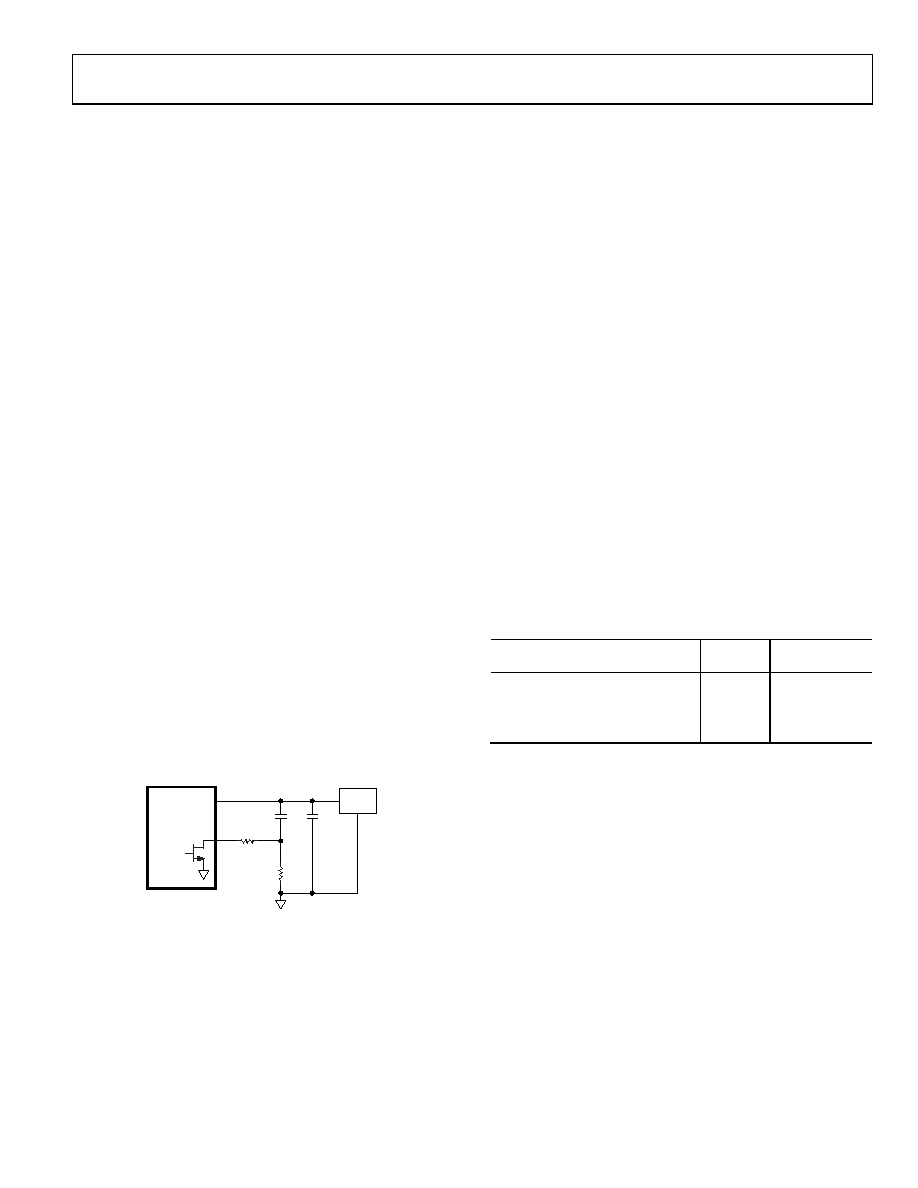
resistor (R1A) in parallel with the damping resistor in the loop
filter (see Figure 16). MUXOUT needs to be set to the fastlock
switch to use the internal switch. For example, if the charge
pump current is increased by 16, the damping resistor, R1,
needs to be decreased by while in wide bandwidth mode.
ADF4153
VCO
C2
C1
CP
FL
MUXOUT
R1
R1A
03685-
029
Figure 16. ADF4153 with Fastlock
The value of R1A is then chosen so that the total parallel
resistance of R1 and R1A equals 1/4 of R1 alone. This gives
an overall 4× increase in loop bandwidth, while maintaining
stability in wide bandwidth mode.
When the PLL has locked to the new frequency, the charge
pump is again programmed to the lowest charge pump current
setting by setting the fastlock bit to 0. The internal switch opens
and the damping resistor reverts to its original value. This
narrows the loop bandwidth to its original cutoff frequency
to allow better attenuation of the spurs than the wide-loop
bandwidth.
SPUR MECHANISMS
The following section describes the three different spur mechan-
isms that arise with a fractional-N synthesizer and how to
minimize them in the ADF4153.
Fractional Spurs
The fractional interpolator in the ADF4153 is a third-order Σ-Δ
modulator (SDM) with a modulus (MOD) that is programmable
to any integer value from 2 to 4095. In low spur mode (dither
enabled), the minimum allowed value of MOD is 50. The SDM
is clocked at the PFD reference rate (FPFD) that allows PLL
output frequencies to be synthesized at a channel step
resolution of FPFD/MOD.
In lowest noise mode and low noise and spur mode (dither off),
the quantization noise from the Σ-Δ modulator appears as frac-
tional spurs. The interval between spurs is FPFD/L, where L is the
repeat length of the code sequence in the digital Σ-Δ modulator.
For the third-order modulator used in the ADF4153, the repeat
length depends on the value of MOD, as shown in Table 11.
Table 11. Fractional Spurs with Dither Off
Condition (Dither Off)
Repeat
Length
Spur Interval
If MOD is divisible by 2, but not 3
2 × MOD
Channel step/2
If MOD is divisible by 3, but not 2
3 × MOD
Channel step/3
If MOD is divisible by 6
6 × MOD
Channel step/6
Otherwise
MOD
Channel step
In low spur mode (dither enabled), the repeat length is
extended to 221 cycles, regardless of the value of MOD, which
makes the quantization error spectrum look like broadband
noise. This can degrade the in-band phase noise at the PLL
output by as much as 10 dB. Therefore, for lowest noise, dither
off is a better choice, particularly when the final loop BW is low
enough to attenuate even the lowest frequency fractional spur.
Integer Boundary Spurs
Another mechanism for fractional spur creation is interactions
between the RF VCO frequency and the reference frequency.
When these frequencies are not integer related (which is the
point of a fractional-N synthesizer), spur sidebands appear on
the VCO output spectrum at an offset frequency that corresponds
to the beat note or difference frequency between an integer
multiple of the reference and the VCO frequency.
These spurs are attenuated by the loop filter and are more
noticeable on channels close to integer multiples of the
reference where the difference frequency can be inside the
loop bandwidth, therefore, the name integer boundary spurs.
相关PDF资料 |
PDF描述 |
|---|---|
| ADF4117BRUZ-RL7 | IC PLL RF FREQ SYNTHESZR 16TSSOP |
| ADF4153BRUZ-RL7 | IC FRACTION-N FREQ SYNTH 16TSSOP |
| ADF4154BCPZ-RL7 | IC FRACTION-N FREQ SYNTH 20LFCSP |
| SY10E457JC | IC MUX TRIPLE DIFF 2:1 28-PLCC |
| SY10E256JC | IC MUX/LATCH 3-BIT 4:1 28-PLCC |
相关代理商/技术参数 |
参数描述 |
|---|---|
| ADF4153BRU | 功能描述:IC SYNTH PLL RF F-N FREQ 16TSSOP RoHS:否 类别:集成电路 (IC) >> 时钟/计时 - 时钟发生器,PLL,频率合成器 系列:- 标准包装:1,000 系列:Precision Edge® 类型:时钟/频率合成器 PLL:无 输入:CML,PECL 输出:CML 电路数:1 比率 - 输入:输出:2:1 差分 - 输入:输出:是/是 频率 - 最大:10.7GHz 除法器/乘法器:无/无 电源电压:2.375 V ~ 3.6 V 工作温度:-40°C ~ 85°C 安装类型:表面贴装 封装/外壳:16-VFQFN 裸露焊盘,16-MLF? 供应商设备封装:16-MLF?(3x3) 包装:带卷 (TR) 其它名称:SY58052UMGTRSY58052UMGTR-ND |
| ADF4153BRU-REEL | 制造商:Analog Devices 功能描述:PLL Frequency Synthesizer Single 16-Pin TSSOP T/R |
| ADF4153BRU-REEL7 | 功能描述:IC PLL FREQ SYNTHESIZER 16-TSSOP RoHS:否 类别:集成电路 (IC) >> 时钟/计时 - 时钟发生器,PLL,频率合成器 系列:- 标准包装:1,000 系列:Precision Edge® 类型:时钟/频率合成器 PLL:无 输入:CML,PECL 输出:CML 电路数:1 比率 - 输入:输出:2:1 差分 - 输入:输出:是/是 频率 - 最大:10.7GHz 除法器/乘法器:无/无 电源电压:2.375 V ~ 3.6 V 工作温度:-40°C ~ 85°C 安装类型:表面贴装 封装/外壳:16-VFQFN 裸露焊盘,16-MLF? 供应商设备封装:16-MLF?(3x3) 包装:带卷 (TR) 其它名称:SY58052UMGTRSY58052UMGTR-ND |
| ADF4153BRUZ | 功能描述:IC SYNTH PLL RF F-N FREQ 16TSSOP RoHS:是 类别:集成电路 (IC) >> 时钟/计时 - 时钟发生器,PLL,频率合成器 系列:- 标准包装:2,000 系列:- 类型:PLL 频率合成器 PLL:是 输入:晶体 输出:时钟 电路数:1 比率 - 输入:输出:1:1 差分 - 输入:输出:无/无 频率 - 最大:1GHz 除法器/乘法器:是/无 电源电压:4.5 V ~ 5.5 V 工作温度:-20°C ~ 85°C 安装类型:表面贴装 封装/外壳:16-LSSOP(0.175",4.40mm 宽) 供应商设备封装:16-SSOP 包装:带卷 (TR) 其它名称:NJW1504V-TE1-NDNJW1504V-TE1TR |
| ADF4153BRUZ | 制造商:Analog Devices 功能描述:PHASE LOCK LOOP (PLL) IC |
发布紧急采购,3分钟左右您将得到回复。