- 您现在的位置:买卖IC网 > PDF目录11488 > ADG1408YCPZ-REEL7 (Analog Devices Inc)IC MULTIPLEXER 8X1 16LFCSP PDF资料下载
参数资料
| 型号: | ADG1408YCPZ-REEL7 |
| 厂商: | Analog Devices Inc |
| 文件页数: | 2/20页 |
| 文件大小: | 0K |
| 描述: | IC MULTIPLEXER 8X1 16LFCSP |
| 产品培训模块: | iCMOS™ Switches and Multiplexers for Data Acquisition Power Line Monitoring Switch Fundamentals |
| 标准包装: | 1 |
| 系列: | iCMOS® |
| 功能: | 多路复用器 |
| 电路: | 1 x 8:1 |
| 导通状态电阻: | 8 欧姆 |
| 电压电源: | 单/双电源 |
| 电压 - 电源,单路/双路(±): | 5 V ~ 16.5 V,±2.25 V ~ 8.25 V |
| 电流 - 电源: | 220µA |
| 工作温度: | -40°C ~ 125°C |
| 安装类型: | 表面贴装 |
| 封装/外壳: | 16-VQFN 裸露焊盘,CSP |
| 供应商设备封装: | 16-LFCSP-VQ |
| 包装: | 标准包装 |
| 产品目录页面: | 801 (CN2011-ZH PDF) |
| 其它名称: | ADG1408YCPZ-REEL7DKR |
ADG1408/ADG1409
Rev. B | Page 10 of 20
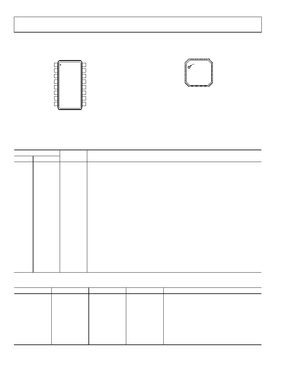
PIN CONFIGURATIONS AND FUNCTION DESCRIPTIONS
1
2
3
4
5
6
7
8
16
15
14
13
12
11
10
9
EN
VSS
S1
S4
S3
S2
A0
A2
GND
VDD
S7
DS
S6
S5
A1
ADG1408
TOP VIEW
(Not to Scale)
8
0
48
61
-00
2
Figure 2. ADG1408 Pin Configuration (TSSOP)
PIN 1
INDICATOR
1
VSS
NOTES
1. THE EXPOSED PAD IS
CONNECTED INTERNALLY. FOR
INCREASED RELIABILITY OF THE
SOLDER JOINTS AND MAXIMUM
THERMAL CAPABILITY, IT IS
RECOMMENDED THAT THE PAD BE
SOLDERED TO THE SUBSTRATE, VSS.
2
S1
3
S2
4
S3
11 VDD
12 GND
10 S5
9S6
5
S
4
6
D
7
S
8
S
7
15
A
0
16
E
N
14
A
1
13
A
2
TOP VIEW
(Not to Scale)
ADG1408
04
86
1-
0
03
Figure 3. ADG1408 Pin Configuration (LFCSP)
Table 8. ADG1408 Pin Function Descriptions
Pin No.
TSSOP
LFCSP
Mnemonic
Description
1
15
A0
Logic Control Input.
2
16
EN
Active High Digital Input. When low, the device is disabled and all switches are off. When high,
Ax logic inputs determine on switches.
3
1
VSS
Most Negative Power Supply Potential. In single supply applications, it can be connected
to ground.
4
2
S1
Source Terminal 1. Can be an input or an output.
5
3
S2
Source Terminal 2. Can be an input or an output.
6
4
S3
Source Terminal 3. Can be an input or an output.
7
5
S4
Source Terminal 4. Can be an input or an output.
8
6
D
Drain Terminal. Can be an input or an output.
9
7
S8
Source Terminal 8. Can be an input or an output.
10
8
S7
Source Terminal 7. Can be an input or an output.
11
9
S6
Source Terminal 6. Can be an input or an output.
12
10
S5
Source Terminal 5. Can be an input or an output.
13
11
VDD
Most Positive Power Supply Potential.
14
12
GND
Ground (0 V) Reference.
15
13
A2
Logic Control Input.
16
14
A1
Logic Control Input.
EP
Exposed Pad
The exposed pad is connected internally. For increased reliability of the solder joints and
maximum thermal capability, it is recommended that the pad be soldered to the substrate, VSS.
Table 9. ADG1408 Truth Table
A2
A1
A0
EN
On Switch
X
0
None
0
1
0
1
2
0
1
0
1
3
0
1
4
1
0
1
5
1
0
1
6
1
0
1
7
1
8
相关PDF资料 |
PDF描述 |
|---|---|
| ADG1234YCPZ-REEL7 | IC SWITCH QUAD SPDT 20LFCSP |
| ADG752BRMZ | IC VIDEO SWITCH SPDT 8MSOP |
| ADG212AKNZ | IC SWITCH QUAD SPST 16DIP |
| ADG211AKNZ | IC SWITCH QUAD SPST 16DIP |
| ADG211AKRZ-REEL7 | IC SWITCH QUAD SPST 16SOIC |
相关代理商/技术参数 |
参数描述 |
|---|---|
| ADG1408YRU | 制造商:Analog Devices 功能描述:ANLG MUX SGL 8:1 16.5V/16.5V 16TSSOP - Bulk |
| ADG1408YRUZ | 功能描述:IC MULTIPLEXER 8X1 16TSSOP RoHS:是 类别:集成电路 (IC) >> 接口 - 模拟开关,多路复用器,多路分解器 系列:iCMOS® 特色产品:MicroPak? 标准包装:1 系列:- 功能:开关 电路:2 x SPST - NC 导通状态电阻:500 毫欧 电压电源:单电源 电压 - 电源,单路/双路(±):1.4 V ~ 4.3 V 电流 - 电源:150nA 工作温度:-40°C ~ 125°C 安装类型:表面贴装 封装/外壳:8-XFDFN 供应商设备封装:8-XSON,SOT833-1 (1.95x1) 包装:Digi-Reel® 其它名称:568-5557-6 |
| ADG1408YRUZ-REEL | 功能描述:IC MULTIPLEXER 8X1 16TSSOP RoHS:是 类别:集成电路 (IC) >> 接口 - 模拟开关,多路复用器,多路分解器 系列:iCMOS® 其它有关文件:STG4159 View All Specifications 标准包装:5,000 系列:- 功能:开关 电路:1 x SPDT 导通状态电阻:300 毫欧 电压电源:双电源 电压 - 电源,单路/双路(±):±1.65 V ~ 4.8 V 电流 - 电源:50nA 工作温度:-40°C ~ 85°C 安装类型:表面贴装 封装/外壳:7-WFBGA,FCBGA 供应商设备封装:7-覆晶 包装:带卷 (TR) |
| ADG1408YRUZ-REEL7 | 功能描述:IC MULTIPLEXER 8X1 16TSSOP RoHS:是 类别:集成电路 (IC) >> 接口 - 模拟开关,多路复用器,多路分解器 系列:iCMOS® 其它有关文件:STG4159 View All Specifications 标准包装:5,000 系列:- 功能:开关 电路:1 x SPDT 导通状态电阻:300 毫欧 电压电源:双电源 电压 - 电源,单路/双路(±):±1.65 V ~ 4.8 V 电流 - 电源:50nA 工作温度:-40°C ~ 85°C 安装类型:表面贴装 封装/外壳:7-WFBGA,FCBGA 供应商设备封装:7-覆晶 包装:带卷 (TR) |
| ADG1409 | 制造商:AD 制造商全称:Analog Devices 功能描述:5з ヌax Ron, 4-/8-Channel 【15V/12V/【5V Multiplexers |
发布紧急采购,3分钟左右您将得到回复。