- 您现在的位置:买卖IC网 > PDF目录11215 > ADG2108YCPZ-REEL7 (Analog Devices Inc)IC CROSSPOINT SWIT 8X10 32LFCSP PDF资料下载
参数资料
| 型号: | ADG2108YCPZ-REEL7 |
| 厂商: | Analog Devices Inc |
| 文件页数: | 13/28页 |
| 文件大小: | 0K |
| 描述: | IC CROSSPOINT SWIT 8X10 32LFCSP |
| 产品培训模块: | Switch Fundamentals |
| 产品变化通告: | Interface Change Notice 12/Apr/2010 |
| 标准包装: | 1 |
| 功能: | 交叉点开关 |
| 电路: | 1 x 8:10 |
| 导通状态电阻: | 50 欧姆 |
| 电压电源: | 单/双电源 |
| 电压 - 电源,单路/双路(±): | 12V,±15V |
| 电流 - 电源: | 50nA |
| 工作温度: | -40°C ~ 125°C |
| 安装类型: | 表面贴装 |
| 封装/外壳: | 32-VFQFN 裸露焊盘,CSP |
| 供应商设备封装: | 32-LFCSP-VQ(5x5) |
| 包装: | 剪切带 (CT) |
| 配用: | EVAL-ADG2108EBZ-ND - BOARD EVAL FOR ADG2108 |
| 其它名称: | ADG2108YCPZ-REEL7CT |
第1页第2页第3页第4页第5页第6页第7页第8页第9页第10页第11页第12页当前第13页第14页第15页第16页第17页第18页第19页第20页第21页第22页第23页第24页第25页第26页第27页第28页
ADG2108
Data Sheet
Rev. B | Page 20 of 28
WRITING TO THE ADG2108
INPUT SHIFT REGISTER
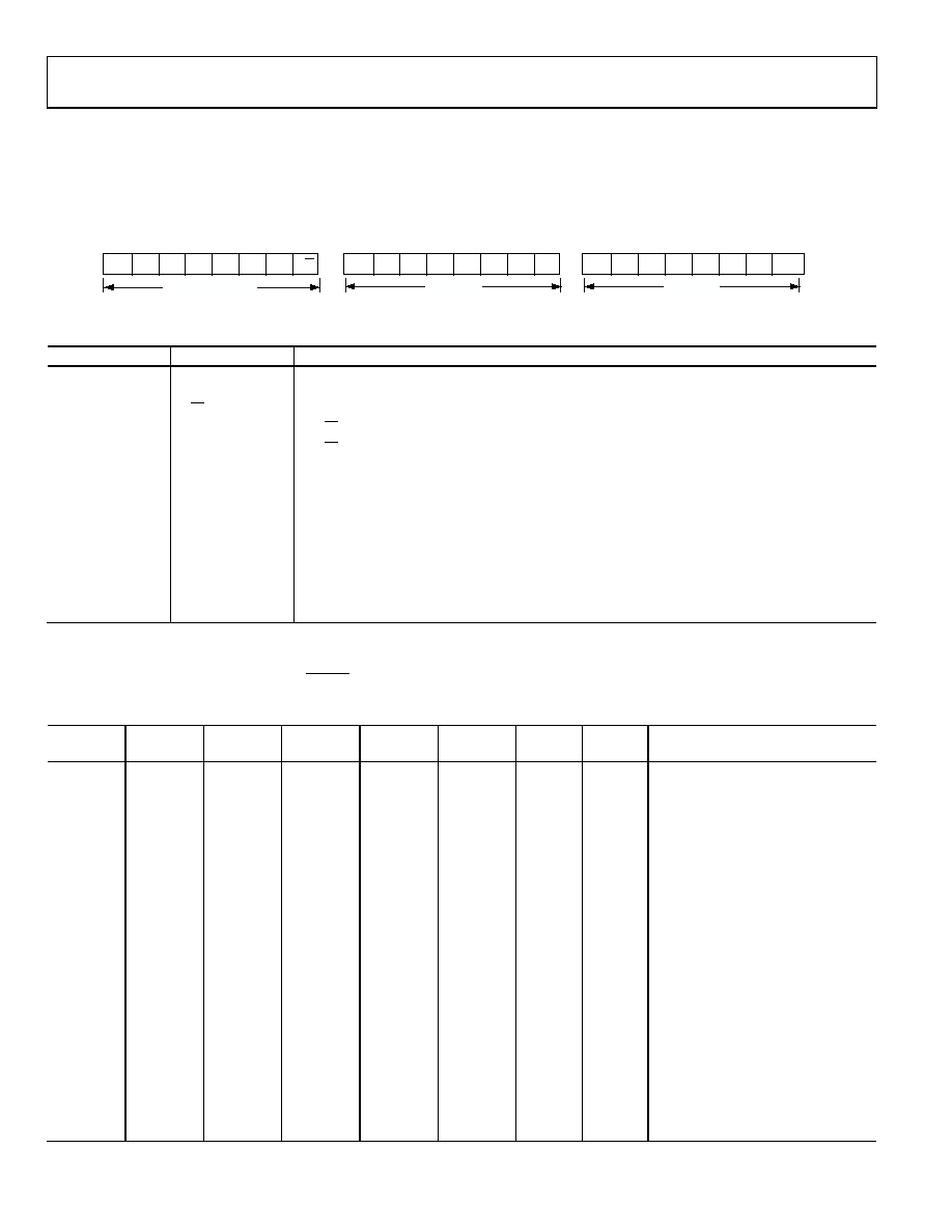
The input shift register is 24 bits wide. A 3-byte write is necessary when writing to this register and is done under the control of the serial
clock input, SCL. The contents of the three bytes of the input shift register are shown in Figure 33 and described in Table 6.
X
LDSW
DB0 (LSB)
DB7 (MSB)
DATA BITS
DATA AX3 AX2
AX1
AX0
AY2
AY1 AY0
DB8 (LSB)
DB15 (MSB)
DATA BITS
1
0
A2
A1
A0
R/W
DB16 (LSB)
DEVICE ADDRESS
DB23 (MSB)
05898-
004
Figure 33. Data-Words
Table 6. Input Shift Register Bit Function Descriptions
Bit
Mnemonic
Descriptions
DB23 to DB17
1110xxx
The MSBs of the ADG2108 are set to 1110. The LSBs of the address byte are set by the state of the
three address pins, Pin A0, Pin A1, and Pin A2.
DB16
R/W
Controls whether the ADG2108 slave device is read from or written to.
If R/W = 1, the ADG2108 is being read from.
If R/W = 0, the ADG2108 is being written to.
DB15
Data
Controls whether the switch is to be opened (off) or closed (on).
If Data = 0, the switch is opened/off.
If Data = 1, the switch is closed/on.
DB14 to DB11
AX3 to AX0
Controls I/Os X0 to X9. See Table 7 for the decode truth table.
DB10 to DB8
AY2 to AY0
Controls I/Os Y0 to Y7. See Table 7 for the decode truth table.
DB7 to DB1
X
Don’t care.
DB0
LDSW
This bit is useful when a number of switches need to be updated simultaneously.
If LDSW = 1, the switch position changes after the new word is read.
If LDSW = 0, the input data is latched, but the switch position is not changed.
As shown in Table 6, Bit DB14 to Bit DB11 control the X input/output lines, while Bit DB10 to Bit DB8 control the Y input/output lines.
Table 7 shows the truth table for these bits. Note that the full coding sequence is written out for Channel Y0, and Channel Y1 to Channel Y7
follow a similar pattern. Note also that the RESET pin must be high when writing to the device.
Table 7. Address Decode Truth Table
DB15
DATA
DB14
AX3
DB13
AX2
DB12
AX1
DB11
AX0
DB10
AY2
DB9
AY1
DB8
AY0
Switch Configuration
X
0
Reserved
X
0
1
0
Reserved
1
0
1
0
X0 to Y0 (on)
0
1
0
X0 to Y0 (off)
1
0
1
0
X1 to Y0 (on)
0
1
0
X1 to Y0 (off)
1
0
1
0
X2 to Y0 (on)
0
1
0
X2 to Y0 (off)
1
0
1
0
1
0
X3 to Y0 (on)
0
1
0
1
0
X3 to Y0 (off)
X
0
1
0
Reserved
X
0
1
0
Reserved
1
0
X4 to Y0 (on)
0
1
0
X4 to Y0 (off)
1
0
1
0
X5 to Y0 (on)
0
1
0
1
0
X5 to Y0 (off)
1
0
1
0
X6 to Y0 (on)
0
1
0
1
0
X6 to Y0 (off)
1
0
1
0
X7 to Y0 (on)
0
1
0
1
0
X7 to Y0 (off)
相关PDF资料 |
PDF描述 |
|---|---|
| ADG426BRSZ-REEL | IC MULTIPLEXER 16X1 28SSOP |
| ADG419TQ | IC SWITCH SPDT 8CDIP |
| VI-JWP-IW | CONVERTER MOD DC/DC 13.8V 100W |
| VE-J30-IW-F2 | CONVERTER MOD DC/DC 5V 100W |
| VI-BWT-IX | CONVERTER MOD DC/DC 6.5V 75W |
相关代理商/技术参数 |
参数描述 |
|---|---|
| ADG211 | 制造商:未知厂家 制造商全称:未知厂家 功能描述:(277.36 k) |
| ADG211A | 制造商:AD 制造商全称:Analog Devices 功能描述:LC2MOS QUAD SPST SWITCHES |
| ADG211A2 | 制造商:未知厂家 制造商全称:未知厂家 功能描述:LC2MOS Quad SPST Switches(277.15 k) |
| ADG211AKN | 功能描述:IC SWITCH QUAD SPST 16DIP RoHS:否 类别:集成电路 (IC) >> 接口 - 模拟开关,多路复用器,多路分解器 系列:LC²MOS 标准包装:1,000 系列:- 功能:多路复用器 电路:1 x 4:1 导通状态电阻:- 电压电源:双电源 电压 - 电源,单路/双路(±):±5V 电流 - 电源:7mA 工作温度:-40°C ~ 85°C 安装类型:表面贴装 封装/外壳:16-SOIC(0.154",3.90mm 宽) 供应商设备封装:16-SOIC 包装:带卷 (TR) |
| ADG211AKNZ | 功能描述:IC SWITCH QUAD SPST 16DIP RoHS:是 类别:集成电路 (IC) >> 接口 - 模拟开关,多路复用器,多路分解器 系列:LC²MOS 特色产品:MicroPak? 标准包装:1 系列:- 功能:开关 电路:2 x SPST - NC 导通状态电阻:500 毫欧 电压电源:单电源 电压 - 电源,单路/双路(±):1.4 V ~ 4.3 V 电流 - 电源:150nA 工作温度:-40°C ~ 125°C 安装类型:表面贴装 封装/外壳:8-XFDFN 供应商设备封装:8-XSON,SOT833-1 (1.95x1) 包装:Digi-Reel® 其它名称:568-5557-6 |
发布紧急采购,3分钟左右您将得到回复。