- 您现在的位置:买卖IC网 > PDF目录2064 > ADG3242BRJ-R2 (Analog Devices Inc)IC SW BUS CTRL 2.5/3.3V SOT23-8 PDF资料下载
参数资料
| 型号: | ADG3242BRJ-R2 |
| 厂商: | Analog Devices Inc |
| 文件页数: | 1/16页 |
| 文件大小: | 0K |
| 描述: | IC SW BUS CTRL 2.5/3.3V SOT23-8 |
| 标准包装: | 1 |
| 类型: | 总线开关 |
| 电路: | 2 x 1:1 |
| 独立电路: | 1 |
| 电压电源: | 单电源 |
| 电源电压: | 2.5V, 3.3V |
| 安装类型: | 表面贴装 |
| 封装/外壳: | SOT-23-8 |
| 供应商设备封装: | SOT-23-8 |
| 包装: | 剪切带 (CT) |
| 其它名称: | ADG3242BRJ-R2CT |
2.5 V/3.3 V, 2-Bit Common Control
Level Translator Bus Switch
ADG3242
Rev. A
Information furnished by Analog Devices is believed to be accurate and reliable. However, no
responsibilityis assumedbyAnalogDevicesforitsuse,norforanyinfringements of patents or other
rightsofthirdpartiesthatmayresultfromitsuse.Specificationssubjecttochangewithoutnotice.No
license is granted by implication or otherwise under any patent or patent rights of Analog Devices.
Trademarksandregisteredtrademarksarethepropertyoftheirrespectiveowners.
One Technology Way, P.O. Box 9106, Norwood, MA 02062-9106, U.S.A.
Tel: 781.329.4700
www.analog.com
Fax: 781.461.3113
2006 Analog Devices, Inc. All rights reserved.
FEATURES
225 ps propagation delay through the switch
4.5 Ω switch connection between ports
Data rate 1.5 Gbps
2.5 V/3.3 V supply operation
Selectable level shifting/translation
Level translation
3.3 V to 2.5 V
3.3 V to 1.8 V
2.5 V to 1.8 V
Small signal bandwidth 710 MHz
8-lead SOT-23 package
APPLICATIONS
3.3 V to 2.5 V voltage translation
3.3 V to 1.8 V voltage translation
2.5 V to 1.8 V voltage translation
Bus switching
Bus isolation
Hot swap
Hot plug
Analog switch applications
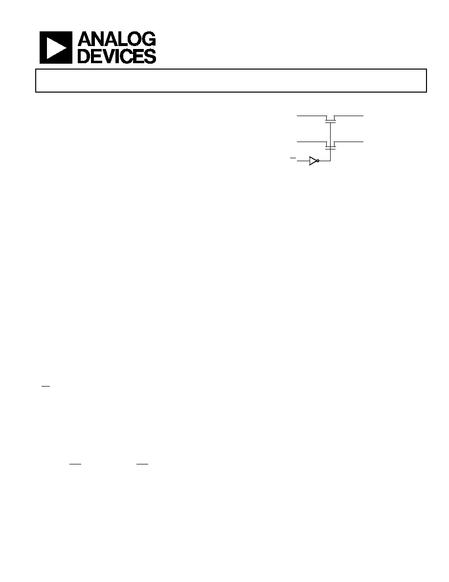
FUNCTIONAL BLOCK DIAGRAM
A1
B1
BE
A0
B0
0
43
09
-00
1
Figure 1.
GENERAL DESCRIPTION
The ADG3242 is a 2.5 V or 3.3 V, 2-bit, 2-port, common control
digital switch. It is designed on a low voltage CMOS process, and
provides low power dissipation, yet gives high switching speed
and very low on resistance. This allows the inputs to be connected
to the outputs without additional propagation delay or generating
additional ground bounce noise.
These switches are enabled by means of a common bus enable
(BE) input signal. This digital switch allows a bidirectional signal
to be switched when on. In the off condition, signal levels up
to the supplies are blocked.
This device is ideal for applications requiring level translation.
When operated from a 3.3 V supply, level translation from 3.3 V
inputs to 2.5 V outputs is allowed. Similarly, if the device is oper-
ated from a 2.5 V supply and 2.5 V inputs are applied, the device
translates the outputs to 1.8 V. In addition, a level translating
select pin (SEL) is included. When SEL is low, VCC is reduced
internally, allowing for level translation between 3.3 V inputs
and 1.8 V outputs. This makes the device suitable for applications
requiring level translation between different supplies, such as
converter to DSP/microcontroller interfacing.
PRODUCT HIGHLIGHTS
1.
3.3 V or 2.5 V supply operation.
2.
Extremely low propagation delay through switch.
3.
4.5 Ω switches connect inputs to outputs.
4.
Level/voltage translation.
5.
Tiny SOT-23 package.
相关PDF资料 |
PDF描述 |
|---|---|
| ADG3243BRJ-R2 | IC SW BUS CTRL 2.5/3.3V SOT23-8 |
| ADG3245BRU | IC SW BUS 2.5/3.3V 8BIT 20TSSOP |
| ADG3246BCPZ-REEL7 | IC SW BUS 10BIT 2.5/3.3V 24LFCSP |
| ADG3247BRU | IC SW BUS 2.5/3.3V 16BIT 38TSSOP |
| ADG3257BRQ-REEL7 | IC MUX QUAD 3.3/5V HS 16-QSOP |
相关代理商/技术参数 |
参数描述 |
|---|---|
| ADG3242BRJ-REEL | 制造商:AD 制造商全称:Analog Devices 功能描述:2.5 V/3.3 V, 2-Bit Common Control Level Translator Bus Switch |
| ADG3242BRJ-REEL7 | 制造商:Analog Devices 功能描述:Bus Switch 1-Element CMOS 2-IN 8-Pin SOT-23 T/R 制造商:Rochester Electronics LLC 功能描述:2.5/3.3V,2 BIT COMMON CTRL,BUS SWITCH IC - Tape and Reel |
| ADG3242BRJZ | 制造商:Analog Devices 功能描述: |
| ADG3242BRJZ-REEL7 | 功能描述:IC SW BUS CTRL 2.5/3.3V SOT23-8 RoHS:是 类别:集成电路 (IC) >> 逻辑 - 信号开关,多路复用器,解码器 系列:- 标准包装:1 系列:74LVC 类型:解码器/多路分解器 电路:1 x 2:4 独立电路:2 输出电流高,低:24mA,24mA 电压电源:单电源 电源电压:1.65 V ~ 3.6 V 工作温度:-40°C ~ 85°C 安装类型:表面贴装 封装/外壳:16-SOIC(0.209",5.30mm 宽) 供应商设备封装:16-SO 包装:Digi-Reel® 其它名称:296-28947-6 |
| ADG3243 | 制造商:AD 制造商全称:Analog Devices 功能描述:2.5 V/3.3 V, 2-Bit, Individual Control Level Translator Bus Switch |
发布紧急采购,3分钟左右您将得到回复。