参数资料
| 型号: | ADG3246BRUZ |
| 厂商: | Analog Devices Inc |
| 文件页数: | 12/12页 |
| 文件大小: | 0K |
| 描述: | IC SW BUS 2.5-3.3V 10BIT 24TSSOP |
| 标准包装: | 62 |
| 类型: | 总线开关 |
| 电路: | 10 x 1:1 |
| 独立电路: | 1 |
| 电压电源: | 单电源 |
| 电源电压: | 2.5V, 3.3V |
| 工作温度: | -40°C ~ 85°C |
| 安装类型: | 表面贴装 |
| 封装/外壳: | 24-TSSOP(0.173",4.40mm 宽) |
| 供应商设备封装: | 24-TSSOP |
| 包装: | 管件 |
REV. 0
ADG3246
–9–
BUS SWITCH APPLICATIONS
Mixed Voltage Operation, Level Translation
Bus switches can be used to provide an ideal solution for interfac-
ing between mixed voltage systems. The ADG3246 is suitable
for applications where voltage translation from 3.3 V technology to
a lower voltage technology is needed. This device can translate
from 3.3 V to 1.8 V, from 2.5 V to 1.8 V, or bidirectionally
from 3.3 V directly to 2.5 V.
Figure 4 shows a block diagram of a typical application in which
a user needs to interface between a 3.3 V ADC and a 2.5 V micro-
processor. The microprocessor may not have 3.3 V tolerant inputs,
therefore placing the ADG3246 between the two devices allows
the devices to communicate easily. The bus switch directly
connects the two blocks, thus introducing minimal propagation
delay, timing skew, or noise.
3.3V ADC
2.5V
3.3V
2.5V
MICROPROCESSOR
ADG3246
3.3V
Figure 4. Level Translation between a 3.3 V ADC
and a 2.5 V Microprocessor
3.3 V to 2.5 V Translation
When VCC is 3.3 V (SEL = VCC) and the input signal range is 0 V
to VCC, the maximum output signal will be clamped to within a
voltage threshold below the VCC supply.
ADG3246
2.5V
3.3V
2.5V
3.3V
Figure 5. 3.3 V to 2.5 V Voltage Translation,
SEL = V
CC
In this case, the output will be limited to 2.5 V, as shown in
Figure 6.
VIN
2.5V
VOUT
0V
3.3V
SWITCH
INPUT
S
WITCH
OU
TPUT
3.3V SUPPLY
SEL = 3.3V
Figure 6. 3.3 V to 2.5 V Voltage Translation,
SEL = V
CC
This device can be used for translation from 2.5 V to 3.3 V
devices and also between two 3.3 V devices.
2.5 V to 1.8 V Translation
When VCC is 2.5 V (SEL = VCC) and the input signal range is 0 V
to VCC, the maximum output signal will, as before, be clamped
to within a voltage threshold below the VCC supply.
ADG3246
1.8V
2.5V
Figure 7. 2.5 V to 1.8 V Voltage Translation,
SEL = V
CC
In this case, the output will be limited to approximately 1.8 V,
as shown in Figure 7.
VIN
1.8V
VOUT
0V
2.5V
SWITCH
INPUT
S
WITCH
OU
TPUT
2.5V SUPPLY
SEL = 2.5V
Figure 8. 2.5 V to 1.8 V Voltage Translation,
SEL = V
CC
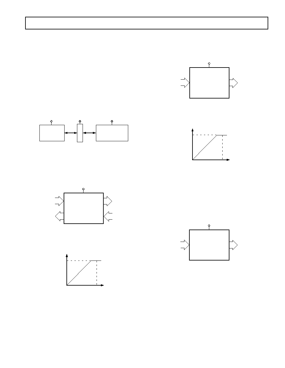
3.3 V to 1.8 V Translation
The ADG3246 offers the option of interfacing between a 3.3 V
device and a 1.8 V device. This is possible through use of the
SEL pin.
SEL pin: An active low control pin. SEL activates internal cir-
cuitry in the ADG3246 that allows voltage translation between
3.3 V devices and 1.8 V devices.
ADG3246
1.8V
3.3V
Figure 9. 3.3 V to 1.8 V Voltage Translation,
SEL = 0 V
When VCC is 3.3 V and the input signal range is 0 V to VCC, the
maximum output signal will be clamped to 1.8 V, as shown in
Figure 9. To do this, the
SEL pin must be tied to Logic 0. If
SEL is unused, it should be tied directly to V
CC.
相关PDF资料 |
PDF描述 |
|---|---|
| MAX196BEAI+ | IC DAS 12BIT 6CH 28-SSOP |
| MAX199BEAI+ | IC DAS 12BIT 8CH 28-SSOP |
| VE-BWP-MX-B1 | CONVERTER MOD DC/DC 13.8V 75W |
| MAX181CEQH+TD | IC DAS 12BIT 100KSPS 44-PLCC |
| ADG3246BCPZ | IC SW BUS 10BIT 2.5/3.3V 24LFCSP |
相关代理商/技术参数 |
参数描述 |
|---|---|
| ADG3246BRUZ-REEL7 | 功能描述:IC SW BUS 2.5-3.3V 10BIT 24TSSOP RoHS:是 类别:集成电路 (IC) >> 逻辑 - 信号开关,多路复用器,解码器 系列:- 标准包装:48 系列:74VHC 类型:多路复用器 电路:4 x 2:1 独立电路:1 输出电流高,低:8mA,8mA 电压电源:单电源 电源电压:2 V ~ 5.5 V 工作温度:-40°C ~ 85°C 安装类型:表面贴装 封装/外壳:16-SOIC(0.154",3.90mm 宽) 供应商设备封装:16-SOIC 包装:管件 |
| ADG3247 | 制造商:AD 制造商全称:Analog Devices 功能描述:2.5 V/3.3 V, 16-Bit, 2-Port Level Translating, Bus Switch |
| ADG3247BCP | 制造商:Analog Devices 功能描述:Bus Switch 2-Element CMOS 16-IN 40-Pin LFCSP EP Tray |
| ADG3247BCP-REEL | 制造商:Analog Devices 功能描述:Bus Switch 2-Element CMOS 16-IN 40-Pin LFCSP EP T/R |
| ADG3247BCP-REEL7 | 制造商:Analog Devices 功能描述:Bus Switch 2-Element CMOS 16-IN 40-Pin LFCSP EP T/R 制造商:Analog Devices 功能描述:BUS SWIT 2-ELEM 8-IN 40LFCSP EP - Tape and Reel |
发布紧急采购,3分钟左右您将得到回复。