参数资料
| 型号: | ADG3248BKS-R2 |
| 厂商: | Analog Devices Inc |
| 文件页数: | 2/12页 |
| 文件大小: | 0K |
| 描述: | IC MUX/DEMUX 2X1 SC70-6 |
| 产品培训模块: | Switch Fundamentals |
| 标准包装: | 1 |
| 功能: | 多路复用器/多路分解器 |
| 电路: | 1 x 2:1 |
| 导通状态电阻: | 12 欧姆 |
| 电压电源: | 单电源 |
| 电压 - 电源,单路/双路(±): | 2.3 V ~ 3.6 V |
| 工作温度: | -40°C ~ 85°C |
| 安装类型: | 表面贴装 |
| 封装/外壳: | 6-TSSOP,SC-88,SOT-363 |
| 供应商设备封装: | SC-70-6 |
| 包装: | 剪切带 (CT) |
| 其它名称: | ADG3248BKS-R2CT |
ADG3248
Rev. A | Page 10 of 12
BUS SWITCH APPLICATIONS
MIXED VOLTAGE OPERATION, LEVEL
TRANSLATION
Bus switches can provide an ideal solution for interfacing between
mixed voltage systems. The ADG3248 is suitable for applications
in which voltage translation from 3.3 V technology to a lower
voltage technology is needed. This device can translate from 2.5 V
to 1.8 V or bidirectionally from 3.3 V directly to 2.5 V.
Figure 20 shows a block diagram of a typical application in
which a user needs to interface between a 3.3 V ADC and a 2.5 V
microprocessor. The microprocessor may not have 3.3 V
tolerant inputs; therefore, placing the ADG3248 between the
two devices allows the devices to communicate easily. The bus
switch directly connects the two blocks, thus introducing
minimal propagation delay, timing skew, or noise.
2.5V
3.3V
A
D
G
3248
3.3V ADC
2.5V
MICROPROCESSOR
04
40
4-
02
0
Figure 20. Level Translation Between a 3.3 V ADC and a 2.5 V Microprocessor
3.3 V to 2.5 V Translation
When VCC is 3.3 V and the input signal range is 0 V to VCC, the
maximum output signal is clamped to within a voltage threshold
below the VCC supply.
In this case, the output is limited to 2.5 V, as shown in Figure 22.
This device can be used for translation from 2.5 V to 3.3 V
devices and also between two 3.3 V devices.
ADG3248
2.5V
3.3V
2.5V
04
40
4-
02
1
Figure 21. 3.3 V to 2.5 V Voltage Translation
2.5V
0V
3.3V
3.3V SUPPLY
VOUT
VIN
SWITCH
INPUT
SW
IT
C
H
OU
TP
U
T
0
440
4-
0
22
Figure 22. 3.3 V to 2.5 V Voltage Translation
2.5 V to 1.8 V Translation
When VCC is 2.5 V and the input signal range is 0 V to VCC, the
maximum output signal is, as before, clamped to within a voltage
threshold below the VCC supply. In this case, the output is limited
to approximately 1.8 V, as shown in Figure 24.
ADG3248
1.8V
2.5V
0
440
4-
0
23
Figure 23. 2.5 V to 1.8 V Voltage Translation
1.8V
0V
2.5V
2.5V SUPPLY
VOUT
VIN
SWITCH
INPUT
SW
IT
C
H
OU
TP
U
T
04
404
-02
4
Figure 24. 2.5 V to 1.8 V Voltage Translation
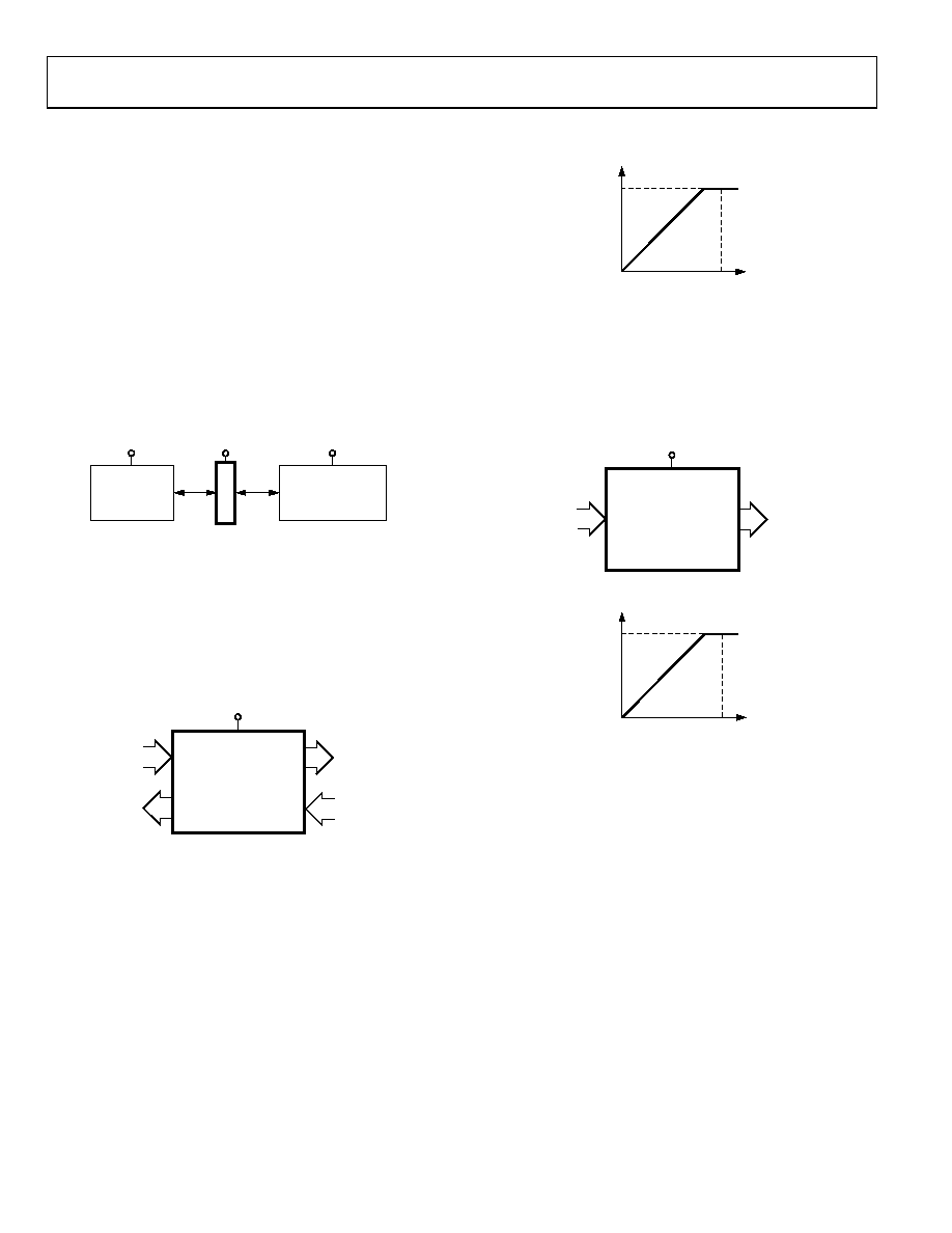
ANALOG SWITCHING
Bus switches can be used in many analog switching applica-
tions, for example, video graphics. Bus switches can have lower
on resistance, smaller on and off channel capacitance, and thus
better frequency performance than their analog counterparts.
The bus switch channel itself, consisting solely of an NMOS
switch, limits the operating voltage (see Figure 3 for a typical
plot) but, in many cases, this does not present an issue.
相关PDF资料 |
PDF描述 |
|---|---|
| ADG3249BRJ-R2 | IC MUX/DEMUX 2X1 SOT23-8 |
| ADG333ABN | IC SWITCH QUAD SPDT 20DIP |
| ADG409BRU | IC MULTIPLEXER DUAL 4X1 16TSSOP |
| ADG412BRU-REEL7 | IC SWITCH QUAD SPST 16TSSOP |
| ADG417BR-REEL | IC SWITCH SPST 8SOIC |
相关代理商/技术参数 |
参数描述 |
|---|---|
| ADG3248BKS-REEL | 制造商:Analog Devices 功能描述:Multiplexer/Demultiplexer Bus Switch 1-Element CMOS 2-IN 6-Pin SC-70 T/R |
| ADG3248BKS-REEL7 | 制造商:Analog Devices 功能描述:Multiplexer/Demultiplexer Bus Switch 1-Element CMOS 2-IN 6-Pin SC-70 T/R 制造商:Rochester Electronics LLC 功能描述: |
| ADG3248BKSZ-REEL7 | 功能描述:IC MUX/DEMUX 2X1 SC70-6 RoHS:是 类别:集成电路 (IC) >> 接口 - 模拟开关,多路复用器,多路分解器 系列:- 特色产品:MicroPak? 标准包装:1 系列:- 功能:开关 电路:2 x SPST - NC 导通状态电阻:500 毫欧 电压电源:单电源 电压 - 电源,单路/双路(±):1.4 V ~ 4.3 V 电流 - 电源:150nA 工作温度:-40°C ~ 125°C 安装类型:表面贴装 封装/外壳:8-XFDFN 供应商设备封装:8-XSON,SOT833-1 (1.95x1) 包装:Digi-Reel® 其它名称:568-5557-6 |
| ADG3248BKZ-REEL7 | 制造商:Analog Devices 功能描述:2.5/3.3V, 2:1 MUX/DEMUX, COMMON CTRL IC. - Tape and Reel |
| ADG3249 | 制造商:AD 制造商全称:Analog Devices 功能描述:2.5 V/3.3 V, 2:1 Multiplexer/ Demultiplexer Bus Switch |
发布紧急采购,3分钟左右您将得到回复。