- 您现在的位置:买卖IC网 > PDF目录11500 > ADG3248BKSZ-REEL7 (Analog Devices Inc)IC MUX/DEMUX 2X1 SC70-6 PDF资料下载
参数资料
| 型号: | ADG3248BKSZ-REEL7 |
| 厂商: | Analog Devices Inc |
| 文件页数: | 1/12页 |
| 文件大小: | 0K |
| 描述: | IC MUX/DEMUX 2X1 SC70-6 |
| 产品培训模块: | iCMOS™ Switches and Multiplexers for Data Acquisition Switch Fundamentals |
| 标准包装: | 1 |
| 功能: | 多路复用器/多路分解器 |
| 电路: | 1 x 2:1 |
| 导通状态电阻: | 12 欧姆 |
| 电压电源: | 单电源 |
| 电压 - 电源,单路/双路(±): | 2.3 V ~ 3.6 V |
| 工作温度: | -40°C ~ 85°C |
| 安装类型: | 表面贴装 |
| 封装/外壳: | 6-TSSOP,SC-88,SOT-363 |
| 供应商设备封装: | SC-70-6 |
| 包装: | 标准包装 |
| 产品目录页面: | 801 (CN2011-ZH PDF) |
| 其它名称: | ADG3248BKSZ-REEL7DKR |
2.5 V/3.3 V, 2:1 Multiplexer/
Demultiplexer Bus Switch
ADG3248
Rev. A
Information furnished by Analog Devices is believed to be accurate and reliable. However, no
responsibilityis assumedbyAnalogDevicesforitsuse,norforanyinfringements of patents or other
rightsofthirdpartiesthatmayresultfromitsuse.Specificationssubjecttochangewithoutnotice.No
license is granted by implication or otherwise under any patent or patent rights of Analog Devices.
Trademarksandregisteredtrademarksarethepropertyoftheirrespectiveowners.
One Technology Way, P.O. Box 9106, Norwood, MA 02062-9106, U.S.A.
Tel: 781.329.4700
www.analog.com
Fax: 781.461.3113
2003–2007 Analog Devices, Inc. All rights reserved.
FEATURES
225 ps propagation delay through the switch
4.5 Ω switch connection between ports
Data rate 1.244 Gbps
2.5 V/3.3 V supply operation
Level translation
3.3 V to 2.5 V
2.5 V to 1.8 V
Small signal bandwidth 610 MHz
6-lead SC70 package
APPLICATIONS
3.3 V to 2.5 V voltage translation
2.5 V to 1.8 V voltage translation
Bus switching
Docking stations
Memory switching
Analog switch applications
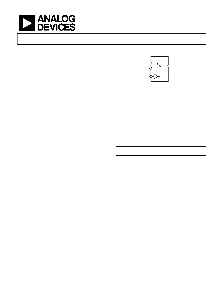
FUNCTIONAL BLOCK DIAGRAM
0
44
04
-00
1
IN
ADG3248
A0
A1
B
NOTES
1. SWITCHES SHOWN FOR A LOGIC 0 INPUT
Figure 1.
GENERAL DESCRIPTION
The ADG3248 is a 2.5 V or 3.3 V, high performance 2:1
multiplexer/demultiplexer. It is designed on a low voltage
CMOS process, which provides low power dissipation yet gives
high switching speed and very low on resistance. The low on
resistance allows the input to be connected to the output
without additional propagation delay or generating additional
ground bounce noise.
Each switch of the ADG3248 conducts equally well in both
directions when on. The ADG3248 exhibits break-before-make
switching action, preventing momentary shorting when
switching channels.
The ADG3248 is available in a tiny 6-lead SC70 package.
Table 1. ADG3248 Truth Table
IN Pin Logic Level
Function
Low (L)
B = A0
High (H)
B = A1
PRODUCT HIGHLIGHTS
1.
3.3 V or 2.5 V supply operation.
2.
Extremely low propagation delay through switch.
3.
4.5 Ω switches connect inputs to outputs.
4.
Tiny SC70 package.
相关PDF资料 |
PDF描述 |
|---|---|
| VI-B34-CU-F3 | CONVERTER MOD DC/DC 48V 200W |
| BH76333FVM-TR | IC VIDEO SIGNAL SWITCHERS 8MSOP |
| PIC18LF45K22-E/ML | MCU 32KB FLASH 1536B RAM 44QFN |
| VI-B34-CU-F2 | CONVERTER MOD DC/DC 48V 200W |
| BH76332FVM-TR | IC VIDEO SIGNAL SWITCHERS 8MSOP |
相关代理商/技术参数 |
参数描述 |
|---|---|
| ADG3248BKZ-REEL7 | 制造商:Analog Devices 功能描述:2.5/3.3V, 2:1 MUX/DEMUX, COMMON CTRL IC. - Tape and Reel |
| ADG3249 | 制造商:AD 制造商全称:Analog Devices 功能描述:2.5 V/3.3 V, 2:1 Multiplexer/ Demultiplexer Bus Switch |
| ADG3249BRJ-R2 | 功能描述:IC MUX/DEMUX 2X1 SOT23-8 RoHS:否 类别:集成电路 (IC) >> 接口 - 模拟开关,多路复用器,多路分解器 系列:- 标准包装:1,000 系列:- 功能:多路复用器 电路:1 x 4:1 导通状态电阻:- 电压电源:双电源 电压 - 电源,单路/双路(±):±5V 电流 - 电源:7mA 工作温度:-40°C ~ 85°C 安装类型:表面贴装 封装/外壳:16-SOIC(0.154",3.90mm 宽) 供应商设备封装:16-SOIC 包装:带卷 (TR) |
| ADG3249BRJ-REEL | 功能描述:IC MUX/DEMUX 2X1 SOT23-8 RoHS:否 类别:集成电路 (IC) >> 接口 - 模拟开关,多路复用器,多路分解器 系列:- 标准包装:1,000 系列:- 功能:多路复用器 电路:1 x 4:1 导通状态电阻:- 电压电源:双电源 电压 - 电源,单路/双路(±):±5V 电流 - 电源:7mA 工作温度:-40°C ~ 85°C 安装类型:表面贴装 封装/外壳:16-SOIC(0.154",3.90mm 宽) 供应商设备封装:16-SOIC 包装:带卷 (TR) |
| ADG3249BRJ-REEL7 | 功能描述:IC MUX/DEMUX 2X1 SOT23-8 RoHS:否 类别:集成电路 (IC) >> 接口 - 模拟开关,多路复用器,多路分解器 系列:- 标准包装:1,000 系列:- 功能:多路复用器 电路:1 x 4:1 导通状态电阻:- 电压电源:双电源 电压 - 电源,单路/双路(±):±5V 电流 - 电源:7mA 工作温度:-40°C ~ 85°C 安装类型:表面贴装 封装/外壳:16-SOIC(0.154",3.90mm 宽) 供应商设备封装:16-SOIC 包装:带卷 (TR) |
发布紧急采购,3分钟左右您将得到回复。