- 您现在的位置:买卖IC网 > PDF目录11257 > ADG3249BRJ-REEL (Analog Devices Inc)IC MUX/DEMUX 2X1 SOT23-8 PDF资料下载
参数资料
| 型号: | ADG3249BRJ-REEL |
| 厂商: | Analog Devices Inc |
| 文件页数: | 2/12页 |
| 文件大小: | 0K |
| 描述: | IC MUX/DEMUX 2X1 SOT23-8 |
| 产品培训模块: | Switch Fundamentals |
| 标准包装: | 10,000 |
| 功能: | 多路复用器/多路分解器 |
| 电路: | 1 x 2:1 |
| 导通状态电阻: | 12 欧姆 |
| 电压电源: | 单电源 |
| 电压 - 电源,单路/双路(±): | 2.3 V ~ 3.6 V |
| 工作温度: | -40°C ~ 85°C |
| 安装类型: | 表面贴装 |
| 封装/外壳: | SOT-23-8 |
| 供应商设备封装: | SOT-23-8 |
| 包装: | 带卷 (TR) |
REV. 0
–10–
ADG3249
Analog Switching
Bus switches can be used in many analog switching applications,
for example, video graphics. Bus switches can have lower on
resistance, smaller ON and OFF channel capacitance, and thus
improved frequency performance than their analog counterparts.
The bus switch channel itself, consisting solely of an NMOS
switch, limits the operating voltage (see TPC 1 for a typical
plot), but in many cases, this does not present an issue.
Multiplexing
Many systems, such as docking stations and memory banks,
have a large number of common bus signals. Common prob-
lems faced by designers of these systems include
Large delays caused by capacitive loading of the bus
Noise due to simultaneous switching of the address and data
bus signals
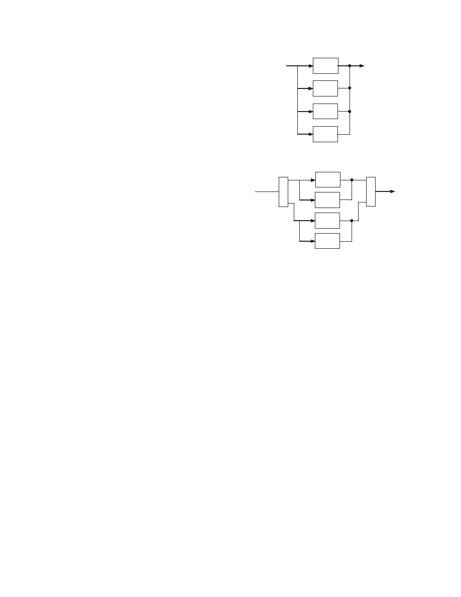
Figure 11 shows an array of memory banks in which each ad-
dress and data signal is loaded by the sum of the individual
loads. If a bus switch is used as shown in Figure 12, the output
load on the memory address and data bits is halved. The speed
at which the selected bank’s data can flow is much improved
because the capacitance loading is halved and the switches
introduce negligible propagation delay. Bus noise is also reduced.
High Impedance during Power-Up/Power-Down
To ensure the high impedance state during power-up or power-
down,
EN should be tied to V
CC through a pull-up resistor; the
minimum value of the resistor is determined by the current-
sinking capability of the driver.
MEMORY
ADDRESS
DATA
MEMORY
BANK B
MEMORY
BANK C
MEMORY
BANK D
MEMORY
BANK A
Figure 11. All Memory Banks Are Permanently
Connected to the Bus
MEMORY
ADDRESS
DATA
MEMORY
BANK B
MEMORY
BANK C
MEMORY
BANK D
MEMORY
BANK A
ADG3249
Figure 12. ADG3249 Used to Reduce Both Access
Time and Noise
相关PDF资料 |
PDF描述 |
|---|---|
| VI-2V3-IX-F2 | CONVERTER MOD DC/DC 24V 75W |
| VI-2V3-IX-F1 | CONVERTER MOD DC/DC 24V 75W |
| VI-2VN-IX-F3 | CONVERTER MOD DC/DC 18.5V 75W |
| VI-2VM-IX-F4 | CONVERTER MOD DC/DC 10V 75W |
| ADG719BRTZ-REEL | IC SWITCH SPDT SOT23-6 |
相关代理商/技术参数 |
参数描述 |
|---|---|
| ADG3249BRJ-REEL7 | 功能描述:IC MUX/DEMUX 2X1 SOT23-8 RoHS:否 类别:集成电路 (IC) >> 接口 - 模拟开关,多路复用器,多路分解器 系列:- 标准包装:1,000 系列:- 功能:多路复用器 电路:1 x 4:1 导通状态电阻:- 电压电源:双电源 电压 - 电源,单路/双路(±):±5V 电流 - 电源:7mA 工作温度:-40°C ~ 85°C 安装类型:表面贴装 封装/外壳:16-SOIC(0.154",3.90mm 宽) 供应商设备封装:16-SOIC 包装:带卷 (TR) |
| ADG3249BRJZ-REEL7 | 功能描述:IC MUX/DEMUX 2X1 SOT23-8 RoHS:是 类别:集成电路 (IC) >> 接口 - 模拟开关,多路复用器,多路分解器 系列:- 标准包装:1,000 系列:- 功能:多路复用器 电路:1 x 4:1 导通状态电阻:- 电压电源:双电源 电压 - 电源,单路/双路(±):±5V 电流 - 电源:7mA 工作温度:-40°C ~ 85°C 安装类型:表面贴装 封装/外壳:16-SOIC(0.154",3.90mm 宽) 供应商设备封装:16-SOIC 包装:带卷 (TR) |
| ADG3257 | 制造商:AD 制造商全称:Analog Devices 功能描述:High Speed, 3.3 V/5 V Quad 2:1 Mux/Demux (4-Bit, 1 of 2) Bus Switch |
| ADG3257BRQ | 功能描述:IC MUX QUAD 3.3/5V HS 16-QSOP RoHS:否 类别:集成电路 (IC) >> 逻辑 - 信号开关,多路复用器,解码器 系列:- 标准包装:48 系列:74VHC 类型:多路复用器 电路:4 x 2:1 独立电路:1 输出电流高,低:8mA,8mA 电压电源:单电源 电源电压:2 V ~ 5.5 V 工作温度:-40°C ~ 85°C 安装类型:表面贴装 封装/外壳:16-SOIC(0.154",3.90mm 宽) 供应商设备封装:16-SOIC 包装:管件 |
| ADG3257BRQ-REEL | 功能描述:IC MUX QUAD 3.3/5V HS 16-QSOP RoHS:否 类别:集成电路 (IC) >> 逻辑 - 信号开关,多路复用器,解码器 系列:- 标准包装:48 系列:74VHC 类型:多路复用器 电路:4 x 2:1 独立电路:1 输出电流高,低:8mA,8mA 电压电源:单电源 电源电压:2 V ~ 5.5 V 工作温度:-40°C ~ 85°C 安装类型:表面贴装 封装/外壳:16-SOIC(0.154",3.90mm 宽) 供应商设备封装:16-SOIC 包装:管件 |
发布紧急采购,3分钟左右您将得到回复。