- 您现在的位置:买卖IC网 > PDF目录8992 > ADG3300BRUZ-REEL7 (Analog Devices Inc)IC XLATOR 8CH 1.2/5.5V 20-TSSOP PDF资料下载
参数资料
| 型号: | ADG3300BRUZ-REEL7 |
| 厂商: | Analog Devices Inc |
| 文件页数: | 7/20页 |
| 文件大小: | 0K |
| 描述: | IC XLATOR 8CH 1.2/5.5V 20-TSSOP |
| 标准包装: | 1 |
| 逻辑功能: | 变换器,双向 |
| 位数: | 8 |
| 输入类型: | 逻辑 |
| 输出类型: | 逻辑 |
| 数据速率: | 50Mbps |
| 通道数: | 8 |
| 输出/通道数目: | 1 |
| 差分 - 输入:输出: | 无/无 |
| 传输延迟(最大): | 6ns |
| 电源电压: | 1.15 V ~ 5.5 V |
| 工作温度: | -40°C ~ 85°C |
| 封装/外壳: | 20-TSSOP(0.173",4.40mm 宽) |
| 供应商设备封装: | 20-TSSOP |
| 包装: | 标准包装 |
| 产品目录页面: | 802 (CN2011-ZH PDF) |
| 其它名称: | ADG3300BRUZ-REEL7DKR |
ADG3300
Rev. 0 | Page 15 of 20
THEORY OF OPERATION
The ADG3300 level translator allows the level shifting necessary
for data transfer in a system where multiple supply voltages are
used. The device requires two supplies, VCCA and VCCY (VCCA ≤
VCCY). These supplies set the logic levels on each side of the
device. When driving the A pins, the device translates the VCCA-
compatible logic levels to VCCY-compatible logic levels available
at the Y pins. Similarly, since the device is capable of bidirectional
translation, when driving the Y pins, the VCCY-compatible logic
levels are translated to VCCA-compatible logic levels available at
the A pins. When EN = 0, the A1 to A8 are internally pulled
down with 6 k resistors while Y1 to Y8 pins are three-stated.
When EN is driven high, the ADG3300 goes into normal
operation mode and performs level translation.
LEVEL TRANSLATOR ARCHITECTURE
The ADG3300 consists of eight bidirectional channels. Each
channel can translate logic levels in either the A Y or the Y A
direction. It uses a one-shot accelerator architecture, which
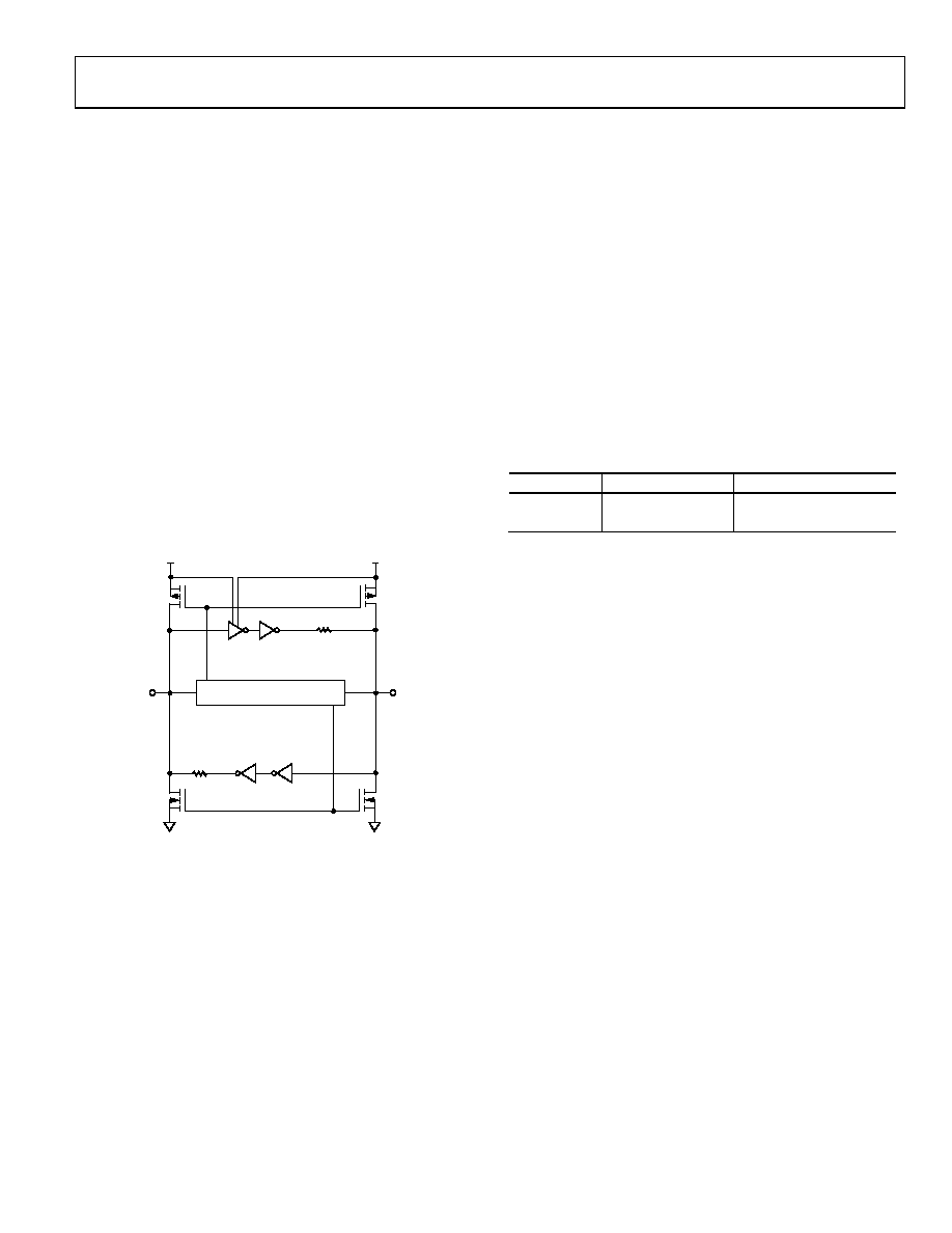
ensures excellent switching characteristics. Figure 35 shows a
simplified block diagram of a bidirectional channel.
ONE-SHOT GENERATOR
6k
6k
Y
VCCA
VCCY
T2
T1
T3
T4
A
05061-037
P
N
U1
U2
U4
U3
Figure 35. Simplified Block Diagram of an ADG3300 Channel
The logic level translation in the A Y direction is performed
using a level translator (U1) and an inverter (U2), and the
translation in the Y A direction is performed using the inverters
U3 and U4. The one-shot generator detects a rising or falling
edge present on either the A side or the Y side of the channel. It
sends a short pulse that turns on the PMOS transistors (T1–T2)
for a rising edge, or the NMOS transistors (T3–T4) for a falling
edge. This charges/discharges the capacitive load faster, which
results in fast rise and fall times.
The inputs of the unused channels (A or Y) should be tied to
their corresponding VCC rail (VCCA or VCCY) or to GND.
INPUT DRIVING REQUIREMENTS
To ensure correct operation of the ADG3300, the circuit that
drives the input of an ADG3300 channels should have an output
impedance of less than or equal to 150 and a minimum
current driving capability of 36 mA.
OUTPUT LOAD REQUIREMENTS
The ADG3300 level translator is designed to drive CMOS-
compatible loads. If current driving capability is required, it is
recommended to use buffers between the ADG3300 outputs
and the load.
ENABLE OPERATION
The ADG3300 provides three-state operation at the Y I/O pins
by using the enable (EN) pin as shown in Table 5.
Table 5. Truth Table
EN
Y I/O Pins
A I/O Pins
0
Hi-Z1
6 k pull-down to GND
1
Normal operation2
1 High impedance state.
2 In normal operation, the ADG3300 performs level translation.
When EN = 0, the ADG3300 enters into three-state mode. In
this mode the current consumption from both the VCCA and
VCCY supplies is reduced, allowing the user to save power, which
is critical, especially for battery-operated systems. The EN input
pin can be driven with either VCCA- or VCCY-compatible logic
levels.
POWER SUPPLIES
For proper operation of the ADG3300, the voltage applied to
the VCCA must always be less than or equal to the voltage applied
to VCCY. To meet this condition, the recommended power-up
sequence is VCCY first and then VCCA. The ADG3300 operates
properly only after both supply voltages reach their nominal
values. It is not recommended to use the part in a system where
VCCA might be greater than VCCY during power-up due to a sig-
nificant increase in the current taken from the VCCA supply. For
optimum performance, the VCCA and VCCY pins should be
decoupled to GND as close as possible to the device.
相关PDF资料 |
PDF描述 |
|---|---|
| VE-J4T-MZ-F3 | CONVERTER MOD DC/DC 6.5V 25W |
| VE-J4T-MZ-F2 | CONVERTER MOD DC/DC 6.5V 25W |
| MS27474E22A2PA | CONN RCPT 85POS JAM NUT W/PINS |
| ADG3308BCPZ-REEL7 | IC XLATOR 8CH 1.2-5.5V 20-LFCSP |
| MS27466T25B4PA | CONN RCPT 56POS WALL MT W/PINS |
相关代理商/技术参数 |
参数描述 |
|---|---|
| ADG3301 | 制造商:AD 制造商全称:Analog Devices 功能描述:Low Voltage 1.15 V to 5.5 V, Single-Channel Bidirectional Logic Level Translator |
| ADG3301BKSZ | 制造商:Analog Devices 功能描述:TRANSLATOR SGL LL BIDIR 6SC-70 制造商:Analog Devices 功能描述:TRANSLATOR, SGL, LL, BIDIR, 6SC-70 制造商:Analog Devices 功能描述:TRANSLATOR, SGL, LL, BIDIR, 6SC-70, No. of Inputs:1, Propagation Delay:6ns, Supp 制造商:Analog Devices 功能描述:TRANSLATOR, SGL, LL, BIDIR, 6SC-70, No. of Inputs:1, Propagation Delay:6ns, Supply Voltage Min:1.15V, Supply Voltage Max:5.5V, Logic Case Style:SC-70, No. of Pins:6, Logic Type:Bidirectional Level Translator, Operating Temperature , RoHS Compliant: Yes |
| ADG3301BKSZ-REEL | 功能描述:IC XLATR BIDIR V-LVL SC70-6 RoHS:是 类别:集成电路 (IC) >> 逻辑 - 变换器 系列:- 产品培训模块:Logic Packages 标准包装:2,500 系列:- 逻辑功能:变换器,双向 位数:2 输入类型:电压 输出类型:电压 数据速率:- 通道数:2 输出/通道数目:1 差分 - 输入:输出:无/无 传输延迟(最大):1.5ns 电源电压:3 V ~ 3.6 V 工作温度:-40°C ~ 85°C 封装/外壳:8-TSSOP,8-MSOP(0.118",3.00mm 宽) 供应商设备封装:8-TSSOP 包装:带卷 (TR) 其它名称:935284857118GTL2002DP/S440-TGTL2002DP/S440-T-ND |
| ADG3301BKSZ-REEL7 | 功能描述:TRANSLATOR SGL LL BIDIR SC70-6 RoHS:是 类别:集成电路 (IC) >> 逻辑 - 变换器 系列:- 标准包装:1 系列:100ELT 逻辑功能:变换器 位数:1 输入类型:TTL 输出类型:差分 数据速率:- 通道数:2 输出/通道数目:1 差分 - 输入:输出:无/是 传输延迟(最大):0.6ns 电源电压:3 V ~ 3.8 V 工作温度:-40°C ~ 85°C 封装/外壳:8-SOIC(0.154",3.90mm 宽) 供应商设备封装:8-SOIC 包装:Digi-Reel® 产品目录页面:1088 (CN2011-ZH PDF) 其它名称:576-1360-6 |
| ADG3304 | 制造商:AD 制造商全称:Analog Devices 功能描述:Low Voltage 1.2 V to 5.5 V, Bidirectional, Logic Level Translators |
发布紧急采购,3分钟左右您将得到回复。