- 您现在的位置:买卖IC网 > PDF目录357567 > ADG432BRZ-REEL (ANALOG DEVICES INC) LC2MOS Precision Quad SPST Switch; Package: SOIC; No of Pins: 16; Temperature Range: Industrial PDF资料下载
参数资料
| 型号: | ADG432BRZ-REEL |
| 厂商: | ANALOG DEVICES INC |
| 元件分类: | 多路复用及模拟开关 |
| 英文描述: | LC2MOS Precision Quad SPST Switch; Package: SOIC; No of Pins: 16; Temperature Range: Industrial |
| 中文描述: | QUAD 1-CHANNEL, SGL POLE SGL THROW SWITCH, PDSO16 |
| 封装: | 0.150 INCH, SOIC-16 |
| 文件页数: | 6/8页 |
| 文件大小: | 131K |
| 代理商: | ADG432BRZ-REEL |
ADG431/ADG432/ADG433
REV. C
–6–
FREQUENCY
–
Hz
120
100
40
100
10M
1k
O
–
10k
100k
1M
80
60
V
DD
= +15V
V
SS
=
–
15V
V
L
= +5V
TPC 7. Off Isolation vs. Frequency
FREQUENCY
–
Hz
110
100
60100
10M
1k
C
–
10k
100k
1M
90
80
70
V
DD
= +15V
V
SS
=
–
15V
V
L
= +5V
TPC 8. Crosstalk vs. Frequency
TRENCH ISOLATION
In the ADG431A, ADG432A and ADG433A, an insulating
oxide layer (trench) is placed between the NMOS and PMOS
transistors of each CMOS switch. Parasitic junctions, which
occur between the transistors in junction isolated switches, are
eliminated, the result being a completely latch-up proof switch.
In junction isolation, the N and P wells of the PMOS and NMOS
transistors from a diode that is reverse-biased under normal
operation. However, during overvoltage conditions, this diode
becomes forward biased. A silicon-controlled rectifier (SCR)
type circuit is formed by the two transistors causing a significant
amplification of the current which, in turn, leads to latch up.
With trench isolation, this diode is removed, the result being a
latch-up proof switch.
BURIED OXIDE LAYER
SUBSTRATE (BACKGATE)
T
R
E
N
C
H
T
R
E
N
C
H
T
R
E
N
C
H
P
+
P
+
P-CHANNEL
N
+
N
+
N-CHANNEL
P
–
N
–
V
G
V
D
V
S
V
G
V
D
V
S
Figure 1. Trench Isolation
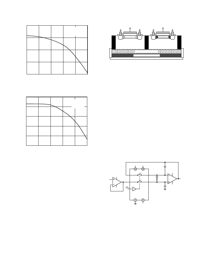
APPLICATION
Figure 2 illustrates a precise, fast sample-and-hold circuit.
An AD845 is used as the input buffer while the output opera-
tional amplifier is an AD711. During the track mode, SW1 is
closed and the output V
OUT
follows the input signal V
IN
. In
the hold mode, SW1 is opened and the signal is held by the
hold capacitor C
H
.
Due to switch and capacitor leakage, the voltage on the hold
capacitor will decrease with time. The ADG431/ADG432/
ADG433 minimizes this droop due to its low leakage specifica-
tions. The droop rate is further minimized by the use of a
polystyrene hold capacitor. The droop rate for the circuit
shown is typically 30
μ
V/
μ
s.
A second switch SW2, which operates in parallel with SW1, is
included in this circuit to reduce pedestal error. Since both
switches will be at the same potential, they will have a differen-
tial effect on the op amp AD711 which will minimize charge
injection effects. Pedestal error is also reduced by the compensa-
tion network R
C
and C
C
. This compensation network also reduces
the hold time glitch while optimizing the acquisition time. Using
the illustrated op amps and component values, the pedestal error
has a maximum value of 5 mV over the
±
10 V input range. Both
the acquisition and settling times are 850 ns.
+15V
–
15V
2200pF
R
C
75
C
1000pF
C
H
2200pF
V
OUT
ADG431
ADG432
ADG433
SW1
SW2
S
S
D
D
+15V
+5V
–
15V
AD845
+15V
–
15V
V
IN
AD711
Figure 2. Fast, Accurate Sample-and-Hold
相关PDF资料 |
PDF描述 |
|---|---|
| ADG433ABR-REEL | LC2MOS Precision Quad SPST Switch; Package: SOIC; No of Pins: 16; Temperature Range: Industrial |
| ADG433ABR-REEL7 | LC2MOS Precision Quad SPST Switch; Package: SOIC; No of Pins: 16; Temperature Range: Industrial |
| ADG433BNZ | LC2MOS Precision Quad SPST Switch; Package: PDIP; No of Pins: 16; Temperature Range: Industrial |
| ADG433BR-REEL | LC2MOS Precision Quad SPST Switch; Package: SOIC; No of Pins: 16; Temperature Range: Industrial |
| ADG433BRZ | LC2MOS Precision Quad SPST Switch; Package: SOIC; No of Pins: 16; Temperature Range: Industrial |
相关代理商/技术参数 |
参数描述 |
|---|---|
| ADG432TQ | 制造商:AD 制造商全称:Analog Devices 功能描述:LC2MOS Precision Quad SPST Switches |
| ADG432TQ/883B | 制造商:未知厂家 制造商全称:未知厂家 功能描述:SPST Analog Switch |
| ADG433 | 制造商:AD 制造商全称:Analog Devices 功能描述:LC2MOS Precision Quad SPST Switches |
| ADG433ABR | 制造商:Analog Devices 功能描述:Analog Switch Quad SPST 16-Pin SOIC N 制造商:Analog Devices 功能描述:IC SWITCH SPST QUAD CMOS |
| ADG433ABR-REEL | 制造商:Analog Devices 功能描述:Analog Switch Quad SPST 16-Pin SOIC N T/R |
发布紧急采购,3分钟左右您将得到回复。