- 您现在的位置:买卖IC网 > PDF目录11479 > ADG507AKRUZ (Analog Devices Inc)IC MULTIPLEXER DUAL 8X1 28TSSOP PDF资料下载
参数资料
| 型号: | ADG507AKRUZ |
| 厂商: | Analog Devices Inc |
| 文件页数: | 4/8页 |
| 文件大小: | 0K |
| 描述: | IC MULTIPLEXER DUAL 8X1 28TSSOP |
| 产品培训模块: | iCMOS™ Switches and Multiplexers for Data Acquisition Switch Fundamentals |
| 标准包装: | 50 |
| 功能: | 多路复用器 |
| 电路: | 2 x 8:1 |
| 导通状态电阻: | 700 欧姆 |
| 电压电源: | 单/双电源 |
| 电压 - 电源,单路/双路(±): | 10.8 V ~ 16.5 V,±5.4 V ~ 8.25 V |
| 电流 - 电源: | 600nA |
| 工作温度: | -40°C ~ 85°C |
| 安装类型: | 表面贴装 |
| 封装/外壳: | 28-TSSOP(0.173",4.40mm 宽) |
| 供应商设备封装: | 28-TSSOP |
| 包装: | 管件 |
| 产品目录页面: | 802 (CN2011-ZH PDF) |
ADG506A/ADG507A
–4–
REV. C
CAUTION
ESD (electrostatic discharge) sensitive device. Electrostatic charges as high as 4000 V readily
accumulate on the human body and test equipment and can discharge without detection.
Although the ADG506A /ADG507A feature proprietary ESD protection circuitry, permanent
damage may occur on devices subjected to high energy electrostatic discharges. Therefore, proper
ESD precautions are recommended to avoid performance degradation or loss of functionality.
ABSOLUTE MAXIMUM RATINGS
1
(TA = 25°C unless otherwise noted)
VDD to VSS
. . . . . . . . . . . . . . . . . . . . . . . . . . . . . . . . . . . 44 V
VDD to GND . . . . . . . . . . . . . . . . . . . . . . . . . . . . . . . . . . 25 V
VSS to GND . . . . . . . . . . . . . . . . . . . . . . . . . . . . . . . . . . –25 V
Analog Inputs
2
Voltage at S, D . . . . . . . . . . . . . . . . . . . . . . . VSS – 2 V to VDD
. . . . . . . . . . . . . . . . . . . . . . . . . . . . . . . . . . . . . . . . + 2 V or
. . . . . . . . . . . . . . . . . . . . . . 20 mA, Whichever Occurs First
Continuous Current, S or D . . . . . . . . . . . . . . . . . . . . . 20 mA
Pulsed Current S or D
1 ms Duration, 10% Duty Cycle . . . . . . . . . . . . . . . . 40 mA
Digital Inputs
2
Voltage at A, EN . . . . . . . . . . . . . . . . . . . . . . . . . . VSS – 4 V
. . . . . . . . . . . . . . . . . . . . . . . . . . . . . . . . . . to VDD + 4 V or
. . . . . . . . . . . . . . . . . . . . . . 20 mA, Whichever Occurs First
Power Dissipation (Any Package)
Up to +75
°C . . . . . . . . . . . . . . . . . . . . . . . . . . . . . 470 mW
Derates above +75
°C by . . . . . . . . . . . . . . . . . . 6 mW/°C
Operating Temperature
Commercial (K Version) . . . . . . . . . . . . . . –40
°C to +85°C
Industrial (B Version) . . . . . . . . . . . . . . . . –40
°C to +85°C
Extended (T Version) . . . . . . . . . . . . . . . –55
°C to +125°C
Storage Temperature Range . . . . . . . . . . . . –65
°C to +150°C
Lead Temperature (Soldering, 10 secs) . . . . . . . . . . . . +300
°C
NOTES
1Stresses above those listed under Absolute Maximum Ratings may cause perma-
nent damage to the device. This is a stress rating only; functional operation of the
device at these or any other conditions above those indicated in the operational
sections of this specification is not implied. Exposure to absolute maximum rating
conditions for extended periods may affect device reliability.
2Overvoltage at A, EN, S or D will be clamped by diodes. Current should be limited
to the Maximum Rating above.
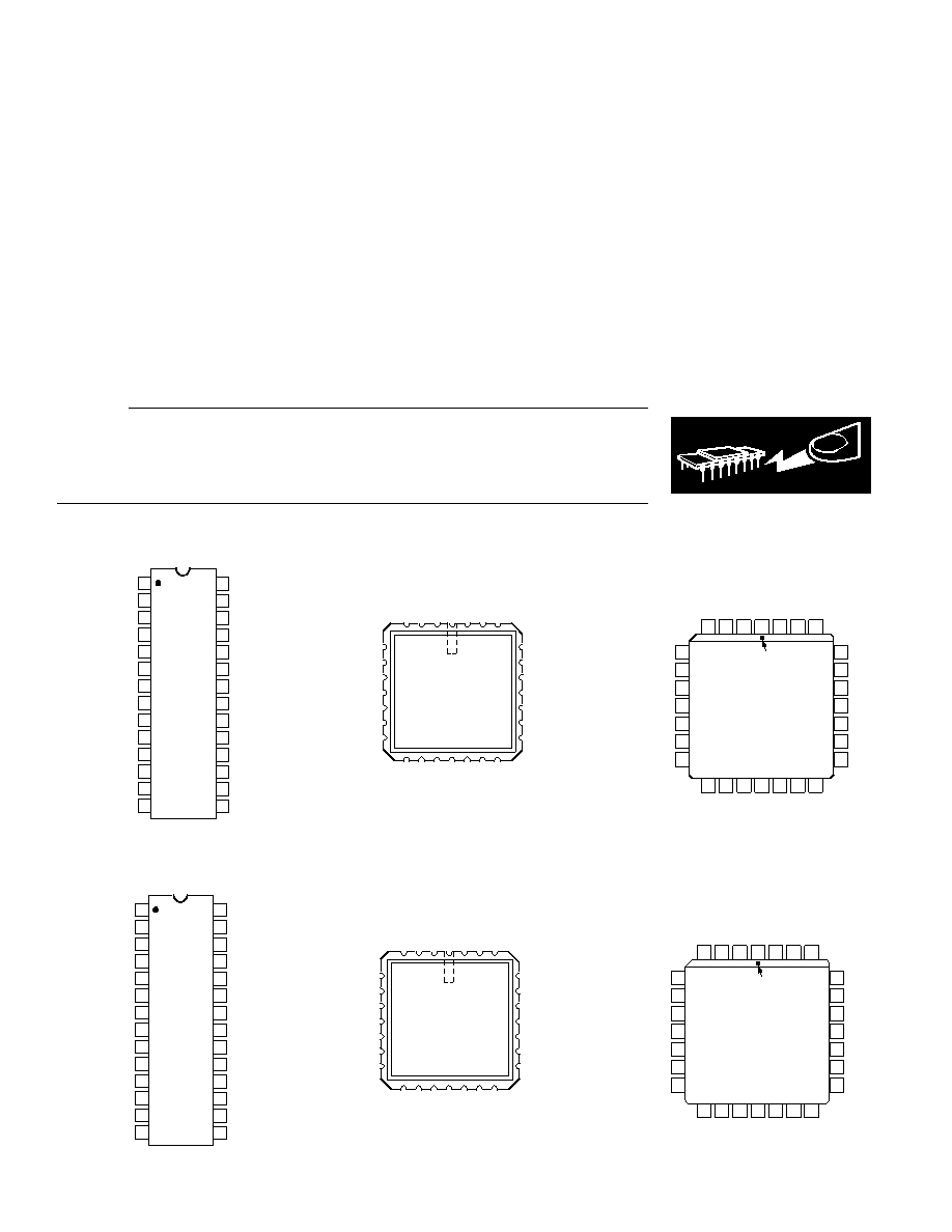
PIN CONFIGURATIONS
DIP, SOIC
14
13
12
11
17
16
15
20
19
18
10
9
8
1
2
3
4
7
6
5
TOP VIEW
(Not to Scale)
28
27
26
25
24
23
22
21
ADG506A
NC = NO CONNECT
VDD
S7
S8
VSS
D
NC
S16
S4
S5
S6
S15
S14
S13
S12
S11
S10
S1
S2
S3
S9
GND
NC
A3
EN
A2
A1
A0
LCCC
28
27
1
2
3
426
25
21
22
23
24
19
20
5
6
7
8
9
10
11
12 13 14 15 16 17 18
TOP VIEW
(Not to Scale)
NC = NO CONNECT
S7A
S6A
S5A
S4A
S3A
S2A
S1A
GND
NC
A1
A0
S8B
NC
DB
V
DD
DA
S8A
EN
S7B
S6B
S5B
S4B
S3B
S2B
S1B
V
SS
ADG507A
A2
NC
PLCC
7
8
9
10
11
5
6
28 27 26
1
2
3
4
21
22
23
24
25
19
20
12
13
14
15
16
17
18
TOP VIEW
(Not to Scale)
PIN 1
IDENTIFIER
S7B
S6B
S5B
S4B
S3B
S7A
S6A
S5A
S4A
S3A
NC = NO CONNECT
ADG507A
S2B
S1B
S2A
S1A
NC
V
DD
A2
A1
A0
V
SS
GND
NC
EN
DB
DA
NC
S8A
S8B
PLCC
7
8
9
10
11
5
6
28 27 26
1
2
3
4
21
22
23
24
25
19
20
12
13
14
15
16
17
18
TOP VIEW
(Not to Scale)
PIN 1
IDENTIFIER
S15
S14
S13
S12
S11
S7
S6
S5
S4
S3
NC = NO CONNECT
ADG506A
S10
S9
S2
S1
NC
V
DD
D
A3
A2
A1
A0
V
SS
S8
GND
NC
EN
S16
DIP, SOIC, TSSOP
14
13
12
11
17
16
15
20
19
18
10
9
8
1
2
3
4
7
6
5
TOP VIEW
(Not to Scale)
28
27
26
25
24
23
22
21
ADG507A
NC = NO CONNECT
VDD
S7A
S8A
VSS
DA
DB
NC
S8B
S4A
S5A
S6A
S7B
S6B
S5B
S4B
S3B
S2B
S1A
S2A
S3A
S1B
GND
NC
EN
A2
A1
A0
LCCC
28
27
1
2
3
426
25
21
22
23
24
19
20
5
6
7
8
9
10
11
12 13 14 15 16 17 18
TOP VIEW
(Not to Scale)
NC = NO CONNECT
S7
S6
S5
S4
S3
S2
S1
GND
NC
A3
A1
A0
EN
S15
S14
S13
S12
S11
S10
S9
S16
NC
V
DD
D
V
SS
S8
ADG506A
A2
WARNING!
ESD SENSITIVE DEVICE
相关PDF资料 |
PDF描述 |
|---|---|
| ADG1634BRUZ | IC SW SPDT 4.5OHM RON 20TSSOP |
| DSPIC33FJ06GS102T-I/MM | IC DSPIC MCU/DSP 6K 28-QFN |
| ADG439FBRZ | IC MULTIPLEXER DUAL 4X1 16SOIC |
| DSPIC30F2012T-30I/SO | IC DSPIC MCU/DSP 12K 28SOIC |
| PIC32MX130F064B-V/SS | IC MCU 32BIT 64KB FLASH 28SSOP |
相关代理商/技术参数 |
参数描述 |
|---|---|
| ADG507AKRUZ | 制造商:Analog Devices 功能描述:IC ANALOG MULTIPLEXER 8 X 1 |
| ADG507AKRUZ-REEL | 制造商:Analog Devices 功能描述:CMOS ? 15 V 8 CHANNEL ANALOG MULTIPLEXER - Tape and Reel |
| ADG507AKRUZ-REEL7 | 制造商:Analog Devices 功能描述:CMOS ? 15 V 8 CHANNEL ANALOG MULTIPLEXER - Tape and Reel |
| ADG507AKRZ | 功能描述:IC MULTIPLEXER DUAL 8X1 28SOIC RoHS:是 类别:集成电路 (IC) >> 接口 - 模拟开关,多路复用器,多路分解器 系列:- 特色产品:MicroPak? 标准包装:1 系列:- 功能:开关 电路:2 x SPST - NC 导通状态电阻:500 毫欧 电压电源:单电源 电压 - 电源,单路/双路(±):1.4 V ~ 4.3 V 电流 - 电源:150nA 工作温度:-40°C ~ 125°C 安装类型:表面贴装 封装/外壳:8-XFDFN 供应商设备封装:8-XSON,SOT833-1 (1.95x1) 包装:Digi-Reel® 其它名称:568-5557-6 |
| ADG507AKRZ | 制造商:Analog Devices 功能描述:Multiplexer IC |
发布紧急采购,3分钟左右您将得到回复。