- 您现在的位置:买卖IC网 > PDF目录11228 > ADG508AKRZ-REEL (Analog Devices Inc)IC MULTIPLEXER 8X1 16SOIC PDF资料下载
参数资料
| 型号: | ADG508AKRZ-REEL |
| 厂商: | Analog Devices Inc |
| 文件页数: | 1/16页 |
| 文件大小: | 0K |
| 描述: | IC MULTIPLEXER 8X1 16SOIC |
| 产品培训模块: | Switch Fundamentals |
| 标准包装: | 2,500 |
| 功能: | 多路复用器 |
| 电路: | 1 x 8:1 |
| 导通状态电阻: | 700 欧姆 |
| 电压电源: | 单/双电源 |
| 电压 - 电源,单路/双路(±): | 10.8 V ~ 16.5 V,±10.8 V ~ 16.5 V |
| 电流 - 电源: | 600µA |
| 工作温度: | -40°C ~ 85°C |
| 安装类型: | 表面贴装 |
| 封装/外壳: | 16-SOIC(0.154",3.90mm 宽) |
| 供应商设备封装: | 16-SOIC |
| 包装: | 带卷 (TR) |
CMOS 4-/8-Channel
Analog Multiplexers
ADG508A/ADG509A
Rev. D
Information furnished by Analog Devices is believed to be accurate and reliable. However, no
responsibilityis assumedbyAnalogDevicesforitsuse,norforanyinfringementsof patentsorother
rightsofthirdpartiesthatmayresultfromitsuse.Specificationssubjecttochangewithoutnotice.No
license is granted by implication or otherwise under any patent or patent rights of Analog Devices.
Trademarksandregisteredtrademarksarethepropertyoftheirrespectiveowners.
One Technology Way, P.O. Box 9106, Norwood, MA 02062-9106, U.S.A.
Tel: 781.329.4700
www.analog.com
Fax: 781.461.3113
2009 Analog Devices, Inc. All rights reserved.
FEATURES
44 V supply maximum rating
VSS to VDD analog signal range
Single-/dual-supply specifications
Wide supply range: 10.8 V to 16.5 V
Extended plastic temperature range: 40°C to +85°C
Low power dissipation: 28 mW maximum
Low leakage: 20 pA typical
Available in 16-lead DIP/SOIC and 20-lead PLCC/LCC
packages
Superior alternative to
DG508A, HI-508
DG509A, HI-509
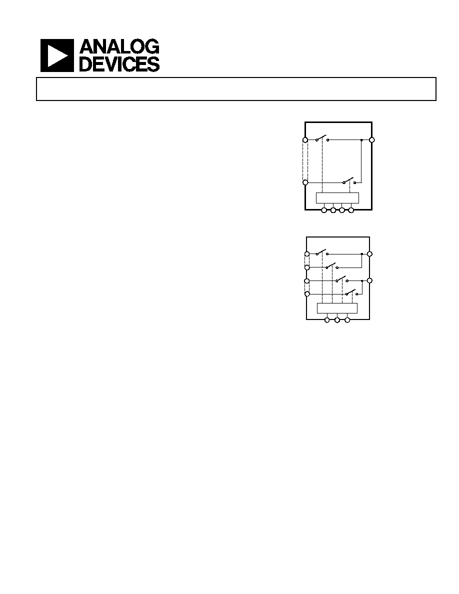
FUNCTIONAL BLOCK DIAGRAMS
ADG508A
S1
S8
D
A0 A1 A2 EN
DECODER
00
05
1-
00
1
Figure 1. ADG508A
ADG509A
S1A
S4A
DA
A0 A1
EN
DECODER
DB
S1B
S4B
00
0
5
1-
0
02
Figure 2. ADG509A
GENERAL DESCRIPTION
The ADG508A and ADG509A are CMOS monolithic analog
multiplexers with eight channels and dual four channels, respec-
tively. The ADG508A switches one of eight inputs to a common
output, depending on the state of three binary addresses and an
enable input. The ADG509A switches one of four differential
inputs to a common differential output, depending on the state
of two binary addresses and an enable input. Both devices have
TTL and 5 V CMOS logic-compatible digital inputs.
The ADG508A and ADG509A are designed on an enhanced
LC2MOS process that gives an increased signal capability of VSS
to VDD and enables operation over a wide range of supply voltages.
The devices can comfortably operate anywhere in the 10.8 V to
16.5 V single- or dual-supply range. These multiplexers also
feature high switching speeds and low RON.
PRODUCT HIGHLIGHTS
1.
Single-/Dual-Supply Specifications with a Wide Tolerance.
The devices are specified in the 10.8 V to 16.5 V range for
both single and dual supplies.
2.
Extended Signal Range. The enhanced LC2MOS processing
results in a high breakdown and an increased analog signal
range of VSS to VDD.
3.
Break-Before-Make Switching. Switches are guaranteed
break-before-make so that input signals are protected
against momentary shorting.
4.
Low Leakage. Leakage currents in the range of 20 pA make
these multiplexers suitable for high precision circuits.
相关PDF资料 |
PDF描述 |
|---|---|
| CDR13BP390EFMS | CAP CER 39PF 500V 1% BP 1111 |
| ADG451BR-REEL7 | IC SWITCH QUAD SPST 16SOIC |
| ADG202AKR | IC SWITCH QUAD SPST 16SOIC |
| M39014/22-0832 | CAP CER 0.1UF 100V 10% RADIAL |
| ADG211AKN | IC SWITCH QUAD SPST 16DIP |
相关代理商/技术参数 |
参数描述 |
|---|---|
| ADG508AKRZ-REEL1 | 制造商:AD 制造商全称:Analog Devices 功能描述:CMOS 4-/8-Channel Analog Multiplexers |
| ADG508AKRZ-REEL7 | 功能描述:IC MULTIPLEXER 8X1 16SOIC RoHS:是 类别:集成电路 (IC) >> 接口 - 模拟开关,多路复用器,多路分解器 系列:- 标准包装:1,000 系列:- 功能:多路复用器 电路:1 x 4:1 导通状态电阻:- 电压电源:双电源 电压 - 电源,单路/双路(±):±5V 电流 - 电源:7mA 工作温度:-40°C ~ 85°C 安装类型:表面贴装 封装/外壳:16-SOIC(0.154",3.90mm 宽) 供应商设备封装:16-SOIC 包装:带卷 (TR) |
| ADG508AKRZ-REEL71 | 制造商:AD 制造商全称:Analog Devices 功能描述:CMOS 4-/8-Channel Analog Multiplexers |
| ADG508ATCHIPS | 制造商:未知厂家 制造商全称:未知厂家 功能描述:8-Channel Analog Multiplexer |
| ADG508ATE | 制造商:AD 制造商全称:Analog Devices 功能描述:CMOS 4/8 CHAANNEL ANALOG MULTIPLEXERS |
发布紧急采购,3分钟左右您将得到回复。