- 您现在的位置:买卖IC网 > PDF目录11493 > ADG509AKRZ-REEL7 (Analog Devices Inc)IC MULTIPLEXER DUAL 4X1 16SOIC PDF资料下载
参数资料
| 型号: | ADG509AKRZ-REEL7 |
| 厂商: | Analog Devices Inc |
| 文件页数: | 15/16页 |
| 文件大小: | 0K |
| 描述: | IC MULTIPLEXER DUAL 4X1 16SOIC |
| 产品培训模块: | iCMOS™ Switches and Multiplexers for Data Acquisition Switch Fundamentals |
| 标准包装: | 1 |
| 功能: | 多路复用器 |
| 电路: | 2 x 4:1 |
| 导通状态电阻: | 700 欧姆 |
| 电压电源: | 单/双电源 |
| 电压 - 电源,单路/双路(±): | 10.8 V ~ 16.5 V,±10.8 V ~ 16.5 V |
| 电流 - 电源: | 600µA |
| 工作温度: | -40°C ~ 85°C |
| 安装类型: | 表面贴装 |
| 封装/外壳: | 16-SOIC(0.154",3.90mm 宽) |
| 供应商设备封装: | 16-SOIC |
| 包装: | 标准包装 |
| 其它名称: | ADG509AKRZ-REEL7DKR |
ADG508A/ADG509A
Rev. D | Page 8 of 16
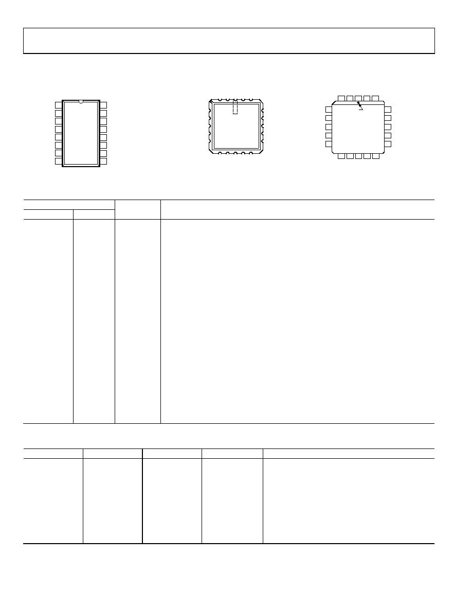
PIN CONFIGURATIONS AND FUNCTION DESCRIPTIONS
A0 1
EN 2
VSS 3
S1 4
A1
16
A2
15
GND
14
VDD
13
S2 5
S3 6
S4 7
S5
12
S6
11
S7
10
D 8
S8
9
ADG508A
TOP VIEW
(Not to Scale)
000
51
-00
3
Figure 3. ADG508A DIP, SOIC
4
VSS
5
S1
6
NC
7
S2
8
S3
18
GND
17
VDD
16
NC
15
S5
14
S6
19
A2
20
A1
1
NC
2
A0
3
EN
13
S7
12
S8
11
NC
10
D
9
S4
ADG508A
TOP VIEW
(Not to Scale)
NC = NO CONNECT
00
05
1-
00
4
Figure 4. ADG508A LCC
120
19
2
3
4
5
6
7
8
18
17
16
15
14
9
10
11
12
13 NC = NO CONNECT
VSS
S1
NC
S2
S3
GND
VDD
NC
S5
S6
EN
A0
NC
A1
A2
S4
D
NC
S8
S7
PIN 1
IDENTIFIER
ADG508A
TOP VIEW
(Not to Scale)
0
051
-00
5
Figure 5. ADG508A PLCC
Table 4. ADG508A Pin Function Description
Pin Number
DIP/SOIC
PLCC/LCC
Mnemonic
Description
1
2
A0
Logic Control Input.
2
3
EN
Active High Digital Input. When low, the device is disabled and all switches are off.
When high, Ax logic inputs determine on switches.
3
4
VSS
Most Negative Power Supply Potential in Dual Supplies. In single-supply applications,
it can be connected to ground.
4
5
S1
Source Terminal 1. Can be an input or an output.
5
7
S2
Source Terminal 2. Can be an input or an output.
6
8
S3
Source Terminal 3. Can be an input or an output.
7
9
S4
Source Terminal 4. Can be an input or an output.
8
10
D
Drain Terminal. Can be an input or an output.
9
12
S8
Source Terminal 8. Can be an input or an output.
10
13
S7
Source Terminal 7. Can be an input or an output.
11
14
S6
Source Terminal 6. Can be an input or an output.
12
15
S5
Source Terminal 5. Can be an input or an output.
13
17
VDD
Most Positive Power Supply Potential.
14
18
GND
Ground (0 V) Reference.
15
19
A2
Logic Control Input.
16
20
A1
Logic Control Input.
N/A
1
NC
No Connect.
N/A
6
NC
No Connect.
N/A
11
NC
No Connect.
N/A
16
NC
No Connect.
Table 5. ADG508A Truth Table
A2
A1
A0
EN
On Switch
X
0
None
0
1
0
1
2
0
1
0
1
3
0
1
4
1
0
1
5
1
0
1
6
1
0
1
7
1
8
1 X = don’t care.
相关PDF资料 |
PDF描述 |
|---|---|
| VE-BNP-CU-F4 | CONVERTER MOD DC/DC 13.8V 200W |
| VE-BNP-CU-F3 | CONVERTER MOD DC/DC 13.8V 200W |
| VE-BNP-CU-F1 | CONVERTER MOD DC/DC 13.8V 200W |
| PIC16C770-I/SS | IC MCU OTP 2KX14 A/D PWM 20SSOP |
| ADG787BRMZ | IC MUX/DEMUX DUAL 2X1 10MSOP |
相关代理商/技术参数 |
参数描述 |
|---|---|
| ADG509AKRZ-REEL71 | 制造商:AD 制造商全称:Analog Devices 功能描述:CMOS 4-/8-Channel Analog Multiplexers |
| ADG509ATCHIPS | 制造商:Analog Devices 功能描述: |
| ADG509ATE | 制造商:AD 制造商全称:Analog Devices 功能描述:CMOS 4/8 CHAANNEL ANALOG MULTIPLEXERS |
| ADG509ATE/883B | 制造商:未知厂家 制造商全称:未知厂家 功能描述:4-Channel Analog Multiplexer |
| ADG509ATQ | 功能描述:IC MULTIPLEXER DUAL 4X1 16CDIP RoHS:否 类别:集成电路 (IC) >> 接口 - 模拟开关,多路复用器,多路分解器 系列:- 其它有关文件:STG4159 View All Specifications 标准包装:5,000 系列:- 功能:开关 电路:1 x SPDT 导通状态电阻:300 毫欧 电压电源:双电源 电压 - 电源,单路/双路(±):±1.65 V ~ 4.8 V 电流 - 电源:50nA 工作温度:-40°C ~ 85°C 安装类型:表面贴装 封装/外壳:7-WFBGA,FCBGA 供应商设备封装:7-覆晶 包装:带卷 (TR) |
发布紧急采购,3分钟左右您将得到回复。