- 您现在的位置:买卖IC网 > PDF目录11229 > ADG5209BCPZ-RL7 (Analog Devices Inc)IC MUX 4CH LATCHUP PROOF 16LFCSP PDF资料下载
参数资料
| 型号: | ADG5209BCPZ-RL7 |
| 厂商: | Analog Devices Inc |
| 文件页数: | 3/24页 |
| 文件大小: | 0K |
| 描述: | IC MUX 4CH LATCHUP PROOF 16LFCSP |
| 标准包装: | 1,500 |
| 功能: | 多路复用器 |
| 电路: | 1 x 4:1 |
| 导通状态电阻: | 170 欧姆 |
| 电压电源: | 单/双电源 |
| 电压 - 电源,单路/双路(±): | 9 V ~ 40 V,± 9 V ~ 22 V |
| 电流 - 电源: | 80µA |
| 工作温度: | -40°C ~ 125°C |
| 安装类型: | 表面贴装 |
| 封装/外壳: | 16-WQFN 裸露焊盘,CSP |
| 供应商设备封装: | 16-LFCSP-WQ(4x4) |
| 包装: | 带卷 (TR) |
Data Sheet
ADG5208/ADG5209
Rev. A | Page 11 of 24
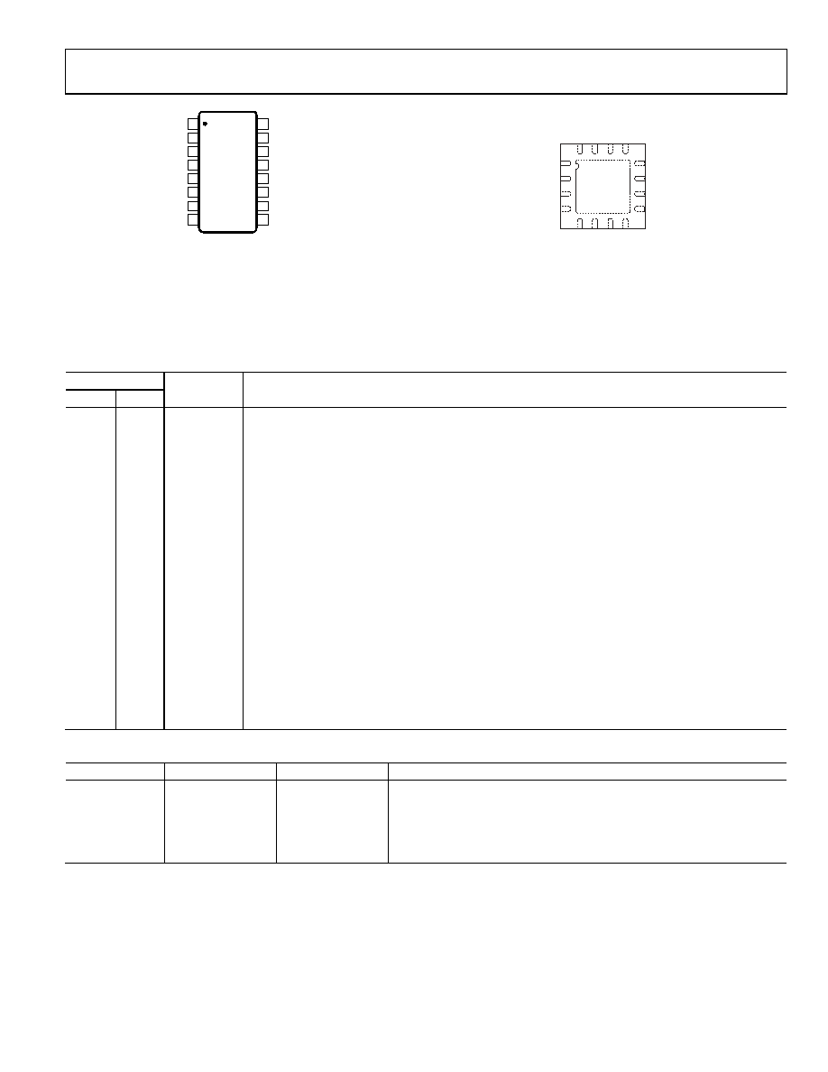
A0
1
EN
2
VSS 3
S1A
4
A1
16
GND
15
VDD
14
S1B
13
S2A
5
S2B
12
S3A
6
S3B
11
S4A
7
S4B
10
DA
8
DB
9
ADG5209
TOP VIEW
(Not to Scale)
09917-
004
Figure 4. ADG5209 Pin Configuration (TSSOP)
12
11
10
1
3
4
VDD
S1B
S2B
9
S3B
VSS
S2A
2
S1A
S3A
6
DA
5
S
4A
7
DB
8
S
4B
16
EN
15
A0
14
A1
13
G
ND
TOP VIEW
(Not to Scale)
ADG5209
NOTES
1. THE EXPOSED PAD IS CONNECTED INTERNALLY. FOR
INCREASED RELIABILITY OF THE SOLDER JOINTS AND
MAXIMUM THERMAL CAPABILITY, IT IS RECOMMENDED
THAT THE PAD BE SOLDERED TO THE SUBSTRATE, VSS.
09917-
005
Figure 5. ADG5209 Pin Configuration (LFCSP)
Table 10. ADG5209 Pin Function Descriptions
Pin No.
TSSOP
LFCSP
Mnemonic
Description
1
15
A0
Logic Control Input.
2
16
EN
Active High Digital Input. When low, the device is disabled and all switches are off. When high,
Ax logic inputs determine the on switches.
3
1
VSS
Most Negative Power Supply Potential. In single-supply applications, this pin can be connected
to ground.
4
2
S1A
Source Terminal 1A. This pin can be an input or an output.
5
3
S2A
Source Terminal 2A. This pin can be an input or an output.
6
4
S3A
Source Terminal 3A. This pin can be an input or an output.
7
5
S4A
Source Terminal 4A. This pin can be an input or an output.
8
6
DA
Drain Terminal A. This pin can be an input or an output.
9
7
DB
Drain Terminal B. This pin can be an input or an output.
10
8
S4B
Source Terminal 4B. This pin can be an input or an output.
11
9
S3B
Source Terminal 3B. This pin can be an input or an output.
12
10
S2B
Source Terminal 2B. This pin can be an input or an output.
13
11
S1B
Source Terminal 1B. This pin can be an input or an output.
14
12
VDD
Most Positive Power Supply Potential.
15
13
GND
Ground (0 V) Reference.
16
14
A1
Logic Control Input.
EP
Exposed Pad
The exposed pad is connected internally. For increased reliability of the solder joints and maximum
thermal capability, it is recommended that the pad be soldered to the substrate, VSS.
Table 11. ADG5209 Truth Table
A1
A0
EN
On Switch Pair
0
None
0
1
0
1
2
1
0
1
3
1
4
1
X is don’t care.
相关PDF资料 |
PDF描述 |
|---|---|
| CKR06BX105KR | CAP CER 1UF 50V 10% RADIAL |
| CDR11BP470AGMS | CAP CER 47PF 50V 2% BP 0605 |
| ADG5208BCPZ-RL7 | IC MUX 8CH LATCHUP PROOF 16LFCSP |
| ADG212AKPZ | IC SWITCH QUAD SPST 20PLCC |
| RPER71H225K8K1C03B | CAP CER 2.2UF 50V 10% RADIAL |
相关代理商/技术参数 |
参数描述 |
|---|---|
| ADG5209BRUZ | 功能描述:IC MULTIPLEXER 5CH 16-TSSOP RoHS:是 类别:集成电路 (IC) >> 接口 - 模拟开关,多路复用器,多路分解器 系列:- 应用说明:Ultrasound Imaging Systems Application Note 产品培训模块:Lead (SnPb) Finish for COTS Obsolescence Mitigation Program 标准包装:250 系列:- 功能:开关 电路:单刀单掷 导通状态电阻:48 欧姆 电压电源:单电源 电压 - 电源,单路/双路(±):2.7 V ~ 5.5 V 电流 - 电源:5µA 工作温度:0°C ~ 70°C 安装类型:表面贴装 封装/外壳:48-LQFP 供应商设备封装:48-LQFP(7x7) 包装:托盘 |
| ADG5209BRUZ-RL7 | 功能描述:IC MULTIPLEXER 1X4:1 16TSSOP RoHS:是 类别:集成电路 (IC) >> 接口 - 模拟开关,多路复用器,多路分解器 系列:- 标准包装:1,000 系列:- 功能:多路复用器 电路:1 x 4:1 导通状态电阻:- 电压电源:双电源 电压 - 电源,单路/双路(±):±5V 电流 - 电源:7mA 工作温度:-40°C ~ 85°C 安装类型:表面贴装 封装/外壳:16-SOIC(0.154",3.90mm 宽) 供应商设备封装:16-SOIC 包装:带卷 (TR) |
| ADG5209FBCPZ-RL7 | 功能描述:IC MULTIPLEXER 4CH 制造商:analog devices inc. 系列:* 零件状态:有效 标准包装:1,500 |
| ADG5209FBRUZ | 功能描述:IC MULTIPLEXER 5CH 16-TSSOP 制造商:analog devices inc. 系列:- 包装:管件 零件状态:在售 开关电路:SP4T 多路复用器/解复用器电路:4:1 电路数:2 导通电阻(最大值):160 欧姆 通道至通道匹配(ΔRon):3.5 欧姆 电压 -?电源,单(V+):9 V ~ 40 V 电压 - 电源,双(V±):±9 V ~ 22 V 开关时间(Ton, Tof)(最大值):140ns,185ns -3db 带宽:130MHz 电荷注入:0.4pC 沟道电容 (CS(off),CD(off)):2.8pF,17pF 电流 - 漏泄(IS(off))(最大值):100pA 串扰:-90dB @ 1MHz 工作温度:-40°C ~ 125°C(TA) 封装/外壳:16-TSSOP(0.173",4.40mm 宽) 供应商器件封装:16-TSSOP 标准包装:96 |
| ADG5209FBRUZ-RL7 | 功能描述:2 Circuit IC Switch 4:1 160 Ohm 16-TSSOP 制造商:analog devices inc. 系列:- 包装:带卷(TR) 零件状态:有效 开关电路:SP4T 多路复用器/解复用器电路:4:1 电路数:2 导通电阻(最大值):160 欧姆 通道至通道匹配(ΔRon):3.5 欧姆 电压 -?电源,单(V+):9 V ~ 40 V 电压 - 电源,双(V±):±9 V ~ 22 V 开关时间(Ton, Tof)(最大值):140ns,185ns -3db 带宽:130MHz 电荷注入:0.4pC 沟道电容 (CS(off),CD(off)):2.8pF,17pF 电流 - 漏泄(IS(off))(最大值):100pA 串扰:-90dB @ 1MHz 工作温度:-40°C ~ 125°C(TA) 封装/外壳:16-TSSOP(0.173",4.40mm 宽) 供应商器件封装:16-TSSOP 标准包装:1,000 |
发布紧急采购,3分钟左右您将得到回复。