- 您现在的位置:买卖IC网 > PDF目录11357 > ADG5233BRUZ (Analog Devices Inc)IC SWITCH ANALOG 16-TSSOP PDF资料下载
参数资料
| 型号: | ADG5233BRUZ |
| 厂商: | Analog Devices Inc |
| 文件页数: | 2/24页 |
| 文件大小: | 0K |
| 描述: | IC SWITCH ANALOG 16-TSSOP |
| 标准包装: | 96 |
| 功能: | 开关 |
| 电路: | 3 x SPDT |
| 导通状态电阻: | 170 欧姆 |
| 电压电源: | 单/双电源 |
| 电压 - 电源,单路/双路(±): | 9 V ~ 40 V,±9 V ~ 22 V |
| 电流 - 电源: | 80µA |
| 工作温度: | -40°C ~ 125°C |
| 安装类型: | 表面贴装 |
| 封装/外壳: | 16-TSSOP(0.173",4.40mm 宽) |
| 供应商设备封装: | 16-TSSOP |
| 包装: | 管件 |
ADG5233/ADG5234
Rev. 0 | Page 10 of 24
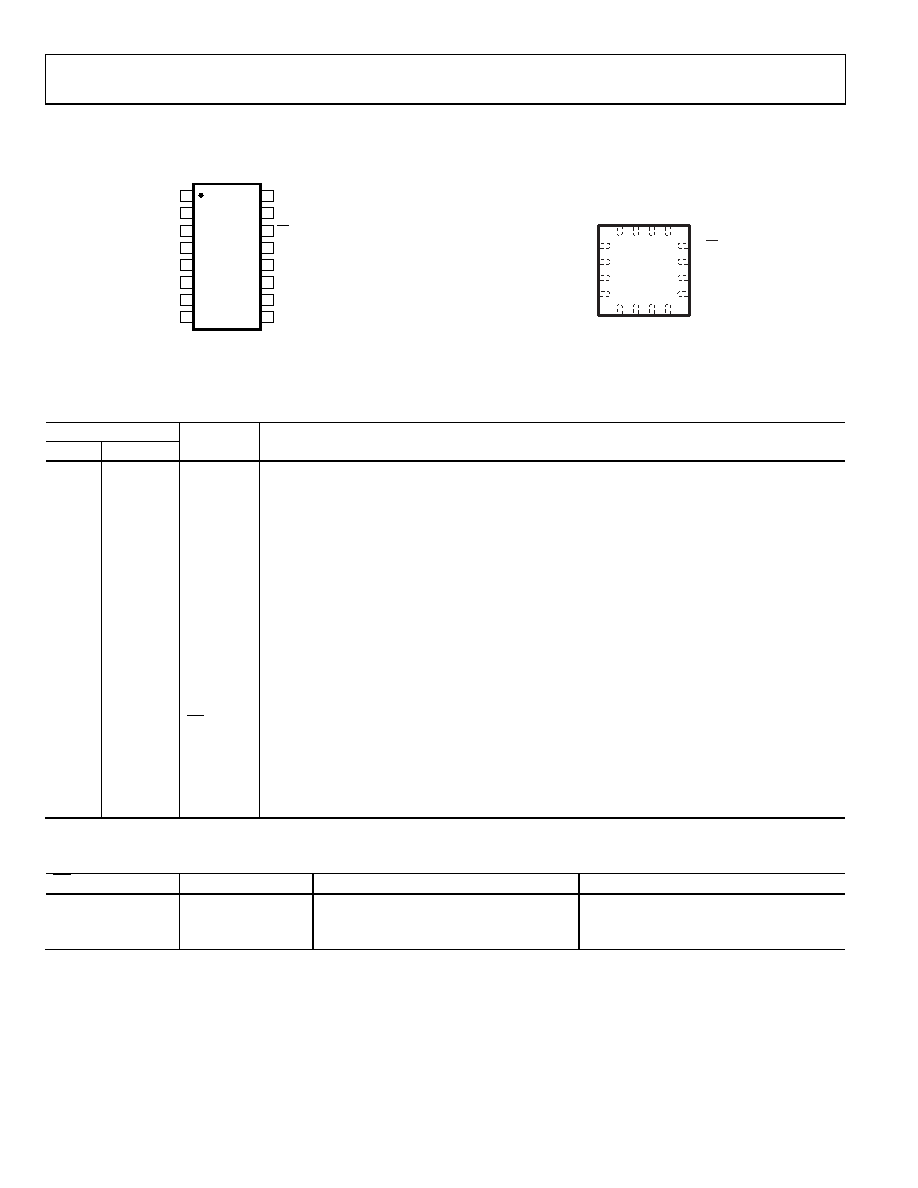
PIN CONFIGURATIONS AND FUNCTION DESCRIPTIONS
VDD 1
S1A
2
D1
3
S1B
4
GND
16
IN1
15
EN
14
VSS
13
S2B
5
S3B
12
D2
6
D3
11
S2A
7
S3A
10
IN2
8
IN3
9
ADG5233
TOP VIEW
(Not to Scale)
09
91
9-
00
3
Figure 3. ADG5233 TSSOP Pin Configuration
NOTES
1. EXPOSED PAD TIED TO SUBSTRATE, VSS.
1
D1
2
S1B
3
S2B
4
D2
11 VSS
12 EN
10 S3B
9D3
5
S
2
A
6
IN
2
7
IN
3
8
S
3
A
1
5
V
D
1
6
S
1
A
1
4
G
N
D
1
3
IN
1
TOP VIEW
(Not to Scale)
ADG5233
0
991
9-
0
04
Figure 4. ADG5233 LFCSP_VQ Pin Configuration
Table 8. ADG5233 Pin Function Descriptions
Pin No.
Mnemonic
Description
TSSOP
LFCSP_VQ
1
15
VDD
Most Positive Power Supply Potential.
2
16
S1A
Source Terminal 1A. This pin can be an input or an output.
3
1
D1
Drain Terminal 1. This pin can be an input or an output.
4
2
S1B
Source Terminal 1B. This pin can be an input or an output.
5
3
S2B
Source Terminal 2B. This pin can be an input or an output.
6
4
D2
Drain Terminal 2. This pin can be an input or an output.
7
5
S2A
Source Terminal 2A. This pin can be an input or an output.
8
6
IN2
Logic Control Input 2.
9
7
IN3
Logic Control Input 3.
10
8
S3A
Source Terminal 3A. This pin can be an input or an output.
11
9
D3
Drain Terminal 3. This pin can be an input or an output.
12
10
S3B
Source Terminal 3B. This pin can be an input or an output.
13
11
VSS
Most Negative Power Supply Potential. In single-supply applications, this pin can be connected to
ground.
14
12
EN
Active Low Digital Input. When high, the device is disabled and all switches are off. When low, INx
logic inputs determine the on switches.
15
13
IN1
Logic Control Input 1.
16
14
GND
Ground (0 V) Reference.
EP
Exposed
Pad
The exposed pad is connected internally. For increased reliability of the solder joints and maximum
thermal capability, it is recommended that the pad be soldered to the substrate, VSS.
Table 9. ADG5233 Truth Table
EN
INx
SxA
SxB
1
Off
0
Off
On
0
1
On
Off
1 X is don’t care.
相关PDF资料 |
PDF描述 |
|---|---|
| PIC18F4523-E/ML | IC PIC MCU FLASH 16KX16 44QFN |
| PIC18F2580T-I/SO | IC PIC MCU FLASH 32KX16 28SOIC |
| DSPIC30F4012-30I/ML | IC DSPIC MCU/DSP 48K 44QFN |
| DSPIC30F4012-20I/ML | IC DSPIC MCU/DSP 48K 44QFN |
| PIC24HJ64GP510-I/PT | IC PIC MCU FLASH 64KB 100TQFP |
相关代理商/技术参数 |
参数描述 |
|---|---|
| ADG5233BRUZ-RL7 | 功能描述:IC SW ANLG TRPL SPDT 16TSSOP RoHS:是 类别:集成电路 (IC) >> 接口 - 模拟开关,多路复用器,多路分解器 系列:- 标准包装:1,000 系列:- 功能:多路复用器 电路:1 x 4:1 导通状态电阻:- 电压电源:双电源 电压 - 电源,单路/双路(±):±5V 电流 - 电源:7mA 工作温度:-40°C ~ 85°C 安装类型:表面贴装 封装/外壳:16-SOIC(0.154",3.90mm 宽) 供应商设备封装:16-SOIC 包装:带卷 (TR) |
| ADG5234 | 制造商:AD 制造商全称:Analog Devices 功能描述:High Voltage Latch-Up Proof |
| ADG5234BCPZ-RL7 | 制造商:Analog Devices 功能描述:LATCHUP PROOF ?20V ?15V +12V +36V 4XSPD - Tape and Reel 制造商:Analog Devices 功能描述:IC SW ANLG QUAD SPDT 20LFCSP 制造商:Analog Devices 功能描述:Latchup Proof 20V 15V +12V +36V 4xSPD |
| ADG5234BRUZ | 功能描述:IC SWITCH ANALOG 20-TSSOP RoHS:是 类别:集成电路 (IC) >> 接口 - 模拟开关,多路复用器,多路分解器 系列:- 应用说明:Ultrasound Imaging Systems Application Note 产品培训模块:Lead (SnPb) Finish for COTS Obsolescence Mitigation Program 标准包装:250 系列:- 功能:开关 电路:单刀单掷 导通状态电阻:48 欧姆 电压电源:单电源 电压 - 电源,单路/双路(±):2.7 V ~ 5.5 V 电流 - 电源:5µA 工作温度:0°C ~ 70°C 安装类型:表面贴装 封装/外壳:48-LQFP 供应商设备封装:48-LQFP(7x7) 包装:托盘 |
| ADG5234BRUZ-RL7 | 功能描述:IC SW ANLG QUAD SPDT 20TSSOP RoHS:是 类别:集成电路 (IC) >> 接口 - 模拟开关,多路复用器,多路分解器 系列:- 其它有关文件:STG4159 View All Specifications 标准包装:5,000 系列:- 功能:开关 电路:1 x SPDT 导通状态电阻:300 毫欧 电压电源:双电源 电压 - 电源,单路/双路(±):±1.65 V ~ 4.8 V 电流 - 电源:50nA 工作温度:-40°C ~ 85°C 安装类型:表面贴装 封装/外壳:7-WFBGA,FCBGA 供应商设备封装:7-覆晶 包装:带卷 (TR) |
发布紧急采购,3分钟左右您将得到回复。