- 您现在的位置:买卖IC网 > PDF目录11222 > ADG659YRU (Analog Devices Inc)IC MULTIPLEXER DUAL 4X1 16TSSOP PDF资料下载
参数资料
| 型号: | ADG659YRU |
| 厂商: | Analog Devices Inc |
| 文件页数: | 3/20页 |
| 文件大小: | 0K |
| 描述: | IC MULTIPLEXER DUAL 4X1 16TSSOP |
| 产品培训模块: | Switch Fundamentals |
| 标准包装: | 96 |
| 功能: | 多路复用器 |
| 电路: | 2 x 4:1 |
| 导通状态电阻: | 150 欧姆 |
| 电压电源: | 单/双电源 |
| 电压 - 电源,单路/双路(±): | 2 V ~ 12 V,±2 V ~ 6 V |
| 电流 - 电源: | 10nA |
| 工作温度: | -40°C ~ 125°C |
| 安装类型: | 表面贴装 |
| 封装/外壳: | 16-TSSOP(0.173",4.40mm 宽) |
| 供应商设备封装: | 16-TSSOP |
| 包装: | 管件 |
ADG658/ADG659
Rev. B | Page 11 of 20
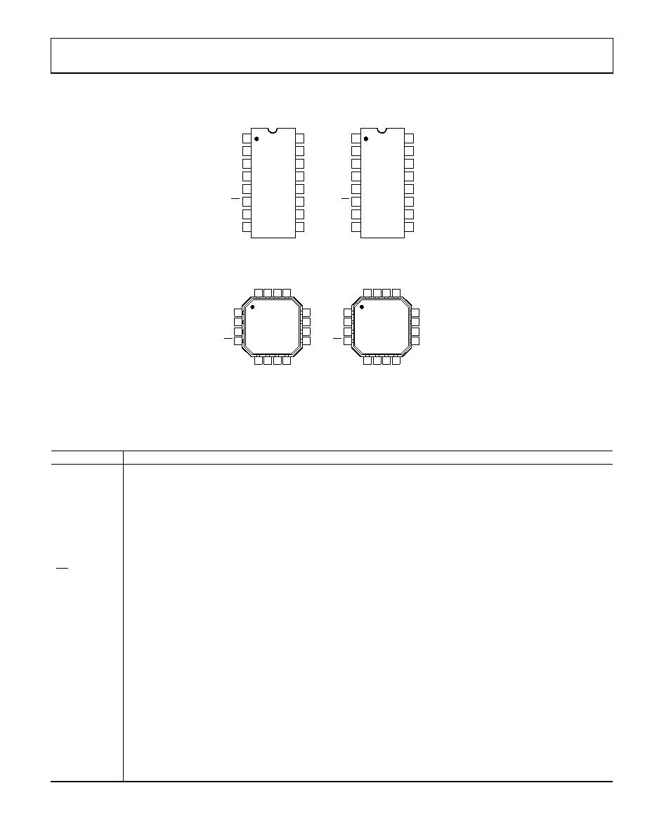
PIN CONFIGURATIONS AND FUNCTION DESCRIPTIONS
ADG659
TOP VIEW
(Not to Scale)
ADG658
TOP VIEW
(Not to Scale)
1
2
3
4
5
6
7
8
1
2
3
4
5
6
7
8
16
15
14
13
12
11
10
9
16
15
14
13
12
11
10
9
VDD
S3
S2
S1
S4
A0
A1
A2
V
DD
S3A
S2A
DA
S1A
S4A
A0
A1
S1B
S3B
DB
S4B
S2B
V
SS
GND
S5
S7
D
S8
S6
VSS
GND
EN
03273-0-002
Figure 2. 16-Lead TSSOP/QSOP Pin Configuration
12
11
10
9
1
2
3
4
16 15 14 13
5
6
7
8
D
S8
S6
V
SS
GND
A2
A1
S2
S1
S4
A0
S7
S5
V
DD
S3
ADG659
TOP VIEW
(Not to Scale)
12
11
10
9
1
2
3
4
16 15 14 13
5
6
7
8
DB
S4B
S2B
V
SS
GND
A1
A0
S2A
DA
S1A
S4A
S3B
S1B
V
DD
S3A
ADG658
TOP VIEW
(Not to Scale)
EN
03273-A
-003
EXPOSED PAD FLOATING
Figure 3. 16-Lead, 4 mm × 4 mm LFCSP Pin Configuration
Table 7. Pin Function Descriptions
Parameter
Description
VDD
Most Positive Power Supply Potential.
VSS
Most Negative Power Supply Potential.
IDD
Positive Supply Current.
ISS
Negative Supply Current.
GND
Ground (0 V) Reference.
S
Source Terminal. May be an input or output.
D
Drain Terminal. May be an input or output.
AX
Logic Control Input.
EN
Active Low Digital Input. When high, device is disabled and all switches are OFF. When low, AX logic inputs determine ON
switch.
VD (VS)
Analog Voltage on Terminals D, S.
RON
Ohmic Resistance between D and S.
RON
On Resistance Match between Any Two Channels, i.e., RONmax RONmin.
RFLAT(ON)
Flatness is defined as the difference between the maximum and minimum value of ON Resistance as measured over the
specified analog signal range.
IS (OFF)
Source Leakage Current with the Switch OFF.
ID (OFF)
Drain Leakage Current with the Switch OFF.
ID, IS (ON)
Channel Leakage Current with the Switch ON.
VINL
Maximum Input Voltage for Logic 0.
VINH
Minimum Input Voltage for Logic 1.
IINL (IINH)
Input Current of the Digital Input.
CS (OFF)
OFF Switch Source Capacitance. Measured with reference to ground.
CD (OFF)
OFF Switch Drain Capacitance. Measured with reference to ground.
CD, CS (ON)
ON Switch Capacitance. Measured with reference to ground.
CIN
Digital Input Capacitance.
相关PDF资料 |
PDF描述 |
|---|---|
| ADG658YRU | IC MULTIPLEXER 8X1 16TSSOP |
| ADG411BR | IC SWITCH QUAD SPST 16SOIC |
| ADG659YRQ | IC MULTIPLEXER DUAL 4X1 16QSOP |
| ADG658YRQ | IC MULTIPLEXER 8X1 16QSOP |
| ADG201AKP | IC SWITCH QUAD SPST 20PLCC |
相关代理商/技术参数 |
参数描述 |
|---|---|
| ADG659YRU-REEL7 | 功能描述:IC MULTIPLEXER DUAL 4X1 16TSSOP RoHS:否 类别:集成电路 (IC) >> 接口 - 模拟开关,多路复用器,多路分解器 系列:- 标准包装:48 系列:- 功能:开关 电路:4 x SPST - NO 导通状态电阻:100 欧姆 电压电源:单/双电源 电压 - 电源,单路/双路(±):2 V ~ 12 V,±2 V ~ 6 V 电流 - 电源:50nA 工作温度:-40°C ~ 85°C 安装类型:表面贴装 封装/外壳:16-SOIC(0.154",3.90mm 宽) 供应商设备封装:16-SOIC 包装:管件 |
| ADG659YRUZ | 功能描述:IC MULTIPLEXER DUAL 4X1 16TSSOP RoHS:是 类别:集成电路 (IC) >> 接口 - 模拟开关,多路复用器,多路分解器 系列:- 特色产品:MicroPak? 标准包装:1 系列:- 功能:开关 电路:2 x SPST - NC 导通状态电阻:500 毫欧 电压电源:单电源 电压 - 电源,单路/双路(±):1.4 V ~ 4.3 V 电流 - 电源:150nA 工作温度:-40°C ~ 125°C 安装类型:表面贴装 封装/外壳:8-XFDFN 供应商设备封装:8-XSON,SOT833-1 (1.95x1) 包装:Digi-Reel® 其它名称:568-5557-6 |
| ADG659YRUZ | 制造商:Analog Devices 功能描述:Analog Switch / Multiplexer (Mux) IC |
| ADG659YRUZ1 | 制造商:AD 制造商全称:Analog Devices 功能描述:3 V/5 V/?±5 V CMOS 4- and 8-Channel Analog Multiplexers |
| ADG659YRUZ-REEL7 | 功能描述:IC MULTIPLEXER DUAL 4X1 16TSSOP RoHS:是 类别:集成电路 (IC) >> 接口 - 模拟开关,多路复用器,多路分解器 系列:- 标准包装:1,000 系列:- 功能:多路复用器 电路:1 x 4:1 导通状态电阻:- 电压电源:双电源 电压 - 电源,单路/双路(±):±5V 电流 - 电源:7mA 工作温度:-40°C ~ 85°C 安装类型:表面贴装 封装/外壳:16-SOIC(0.154",3.90mm 宽) 供应商设备封装:16-SOIC 包装:带卷 (TR) |
发布紧急采购,3分钟左右您将得到回复。