- 您现在的位置:买卖IC网 > PDF目录11248 > ADG721BRM (Analog Devices Inc)IC SWITCH DUAL SPST 8MSOP PDF资料下载
参数资料
| 型号: | ADG721BRM |
| 厂商: | Analog Devices Inc |
| 文件页数: | 4/16页 |
| 文件大小: | 0K |
| 描述: | IC SWITCH DUAL SPST 8MSOP |
| 产品培训模块: | Switch Fundamentals |
| 标准包装: | 50 |
| 功能: | 开关 |
| 电路: | 2 x SPST - NO |
| 导通状态电阻: | 4 欧姆 |
| 电压电源: | 单电源 |
| 电压 - 电源,单路/双路(±): | 1.8 V ~ 5.5 V |
| 电流 - 电源: | 1nA |
| 工作温度: | -40°C ~ 85°C |
| 安装类型: | 表面贴装 |
| 封装/外壳: | 8-TSSOP,8-MSOP(0.118",3.00mm 宽) |
| 供应商设备封装: | 8-MSOP |
| 包装: | 管件 |
ADG721/ADG722/ADG723
Data Sheet
Rev. E | Page 12 of 16
APPLICATIONS
The ADG721/ADG722/ADG723 belong to a new family of
Analog Devices CMOS switches. This series of general-purpose
switches has improved switching times, lower on resistance, higher
bandwidths, low power consumption, and low leakage currents.
ADG721/ADG722/ADG723 SUPPLY VOLTAGES
Functionality of the ADG721/ADG722/ADG723 extends from
a 1.8 V to a 5.5 V single supply, which makes it ideal for battery-
powered instruments, where important design parameters are
power efficiency and performance.
It is important to note that the supply voltage affects the input
signal range, the on resistance, and the switching times of the part.
The typical performance characteristics and the specifications
clearly show the effects of the power supplies.
For VDD = 1.8 V, on resistance is typically 40 Ω over the
temperature range.
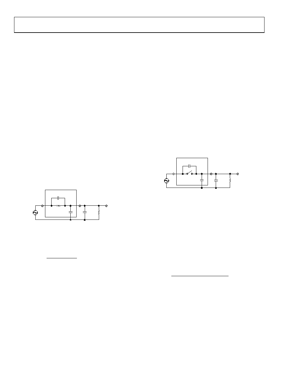
ON RESPONSE VS. FREQUENCY
Figure 21 illustrates the parasitic components that affect the ac
performance of CMOS switches (the switch is shown surrounded
by a box). Additional external capacitances further degrade some
aspects of performance. These capacitances affect feedthrough,
crosstalk, and system bandwidth.
S
D
CD
RLOAD
VOUT
VIN
CDS
CLOAD
RON
00045-
021
Figure 21. Switch Represented by Equivalent Parasitic Components
The transfer function that describes the equivalent diagram of
the switch (Figure 21) is of the form (A)s, as shown in the
following equation:
(
)
(
)
+
=
1
)
(
T
ON
DS
ON
T
R
C
R
s
C
R
s
R
s
A
where:
CT = CLOAD + CD + CDS
RT = RLOAD/(RLOAD + RON)
The signal transfer characteristic is dependent on the switch
channel capacitance, CDS. This capacitance creates a frequency
zero in the numerator of the transfer function A(s). Because the
switch on resistance is small, this zero usually occurs at high
frequencies. The bandwidth is a function of the switch output
capacitance combined with CDS and the load capacitance. The
frequency pole corresponding to these capacitances appears in
the denominator of A(s).
The dominant effect of the output capacitance, CD, causes the
pole breakpoint frequency to occur first. Therefore, in order to
maximize bandwidth, a switch must have a low input and
output capacitance and low on resistance (see Figure 11).
OFF ISOLATION
Off isolation is a measure of the input signal coupled through
an off switch to the switch output. The capacitance, CDS, couples
the input signal to the output load, when the switch is off, as
shown in Figure 22.
S
D
CD
RLOAD
VOUT
VIN
CDS
CLOAD
00045-
022
Figure 22. Off Isolation Is Affected by External Load
Resistance and Capacitance
The larger the value of CDS, the larger the value of feedthrough
produced. Figure 9 illustrates the drop in off isolation as a
function of frequency. From dc to roughly 1 MHz, the switch
shows better than 80 dB isolation. Up to frequencies of 10
MHz, the off isolation remains better than 60 dB. As the
frequency increases, more and more of the input signal is
coupled through to the output. Off isolation can be maximized
by choosing a switch with the smallest CDS possible. The values
of load resistance and capacitance also affect off isolation
because they contribute to the coefficients of the poles and
zeros in the transfer function of the switch when open.
(
)
(
)
(
)
+
=
1
)
(
DS
D
LOAD
DS
LOAD
C
R
s
C
R
s
A
相关PDF资料 |
PDF描述 |
|---|---|
| PIC17C44-33/PT | IC MCU OTP 8KX16 PWM 44TQFP |
| PIC17C44-25/PT | IC MCU OTP 8KX16 PWM 44TQFP |
| ADG713BRU-REEL7 | IC SWITCH QUAD SPST 16TSSOP |
| ADG712BR-REEL7 | IC SWITCH QUAD SPST 16SOIC |
| VI-2WN-IY-S | CONVERTER MOD DC/DC 18.5V 50W |
相关代理商/技术参数 |
参数描述 |
|---|---|
| ADG721BRM | 制造商:Analog Devices 功能描述:SEMICONDUCTOR ((NW)) |
| ADG721BRM-REEL | 功能描述:IC SWITCH DUAL SPST 8MSOP RoHS:否 类别:集成电路 (IC) >> 接口 - 模拟开关,多路复用器,多路分解器 系列:- 标准包装:1,000 系列:- 功能:多路复用器 电路:1 x 4:1 导通状态电阻:- 电压电源:双电源 电压 - 电源,单路/双路(±):±5V 电流 - 电源:7mA 工作温度:-40°C ~ 85°C 安装类型:表面贴装 封装/外壳:16-SOIC(0.154",3.90mm 宽) 供应商设备封装:16-SOIC 包装:带卷 (TR) |
| ADG721BRM-REEL7 | 功能描述:IC SWITCH DUAL SPST 8MSOP RoHS:否 类别:集成电路 (IC) >> 接口 - 模拟开关,多路复用器,多路分解器 系列:- 标准包装:1,000 系列:- 功能:多路复用器 电路:1 x 4:1 导通状态电阻:- 电压电源:双电源 电压 - 电源,单路/双路(±):±5V 电流 - 电源:7mA 工作温度:-40°C ~ 85°C 安装类型:表面贴装 封装/外壳:16-SOIC(0.154",3.90mm 宽) 供应商设备封装:16-SOIC 包装:带卷 (TR) |
| ADG721BRMZ | 功能描述:IC SWITCH DUAL SPST 8MSOP RoHS:是 类别:集成电路 (IC) >> 接口 - 模拟开关,多路复用器,多路分解器 系列:- 特色产品:MicroPak? 标准包装:1 系列:- 功能:开关 电路:2 x SPST - NC 导通状态电阻:500 毫欧 电压电源:单电源 电压 - 电源,单路/双路(±):1.4 V ~ 4.3 V 电流 - 电源:150nA 工作温度:-40°C ~ 125°C 安装类型:表面贴装 封装/外壳:8-XFDFN 供应商设备封装:8-XSON,SOT833-1 (1.95x1) 包装:Digi-Reel® 其它名称:568-5557-6 |
| ADG721BRMZ-AIRBUS | 制造商:Analog Devices 功能描述: |
发布紧急采购,3分钟左右您将得到回复。