- 您现在的位置:买卖IC网 > PDF目录11488 > ADG752BRMZ (Analog Devices Inc)IC VIDEO SWITCH SPDT 8MSOP PDF资料下载
参数资料
| 型号: | ADG752BRMZ |
| 厂商: | Analog Devices Inc |
| 文件页数: | 4/9页 |
| 文件大小: | 0K |
| 描述: | IC VIDEO SWITCH SPDT 8MSOP |
| 产品培训模块: | iCMOS™ Switches and Multiplexers for Data Acquisition Switch Fundamentals |
| 标准包装: | 50 |
| 功能: | 视频开关 |
| 电路: | 1 x SPDT - NC/NO |
| 导通状态电阻: | 18 欧姆 |
| 电压电源: | 单电源 |
| 电压 - 电源,单路/双路(±): | 1.8 V ~ 5.5 V |
| 电流 - 电源: | 1nA |
| 工作温度: | -40°C ~ 85°C |
| 安装类型: | 表面贴装 |
| 封装/外壳: | 8-TSSOP,8-MSOP(0.118",3.00mm 宽) |
| 供应商设备封装: | 8-MSOP |
| 包装: | 管件 |
| 产品目录页面: | 803 (CN2011-ZH PDF) |
ADG752
–4–
Table I. Truth Table
ADG752 IN
Switch S1
Switch S2
0
ON
OFF
1
OFF
ON
CAUTION
ESD (electrostatic discharge) sensitive device. Electrostatic charges as high as 4000 V readily
accumulate on the human body and test equipment and can discharge without detection.
Although the ADG752 features proprietary ESD protection circuitry, permanent damage may
occur on devices subjected to high energy electrostatic discharges. Therefore, proper ESD
precautions are recommended to avoid performance degradation or loss of functionality.
WARNING!
ESD SENSITIVE DEVICE
ABSOLUTE MAXIMUM RATINGS
1
(TA = +25°C unless otherwise noted)
VDD to GND . . . . . . . . . . . . . . . . . . . . . . . . . . . –0.3 V to +6 V
Analog, Digital Inputs2 . . . . . . . . . . . . –0.3 V to VDD +0.3 V or
30 mA, Whichever Occurs First
Peak Current, S or D . . . . . . . . . . . . . . . . . . . . . . . . . . .100 mA
(Pulsed at 1 ms, 10% Duty Cycle Max)
Continuous Current, S or D . . . . . . . . . . . . . . . . . . . . . 30 mA
Operating Temperature Range
Industrial (B Version) . . . . . . . . . . . . . . . . . –40
°C to +85°C
Storage Temperature Range . . . . . . . . . . . . . –65
°C to +150°C
Power Dissipation . . . . . . . . . . . . . . . . . . . . . (TJ Max–TA)/
θJA
Junction Temperature (TJ Max) . . . . . . . . . . . . . . . . . .+150
°C
SOIC Package
θJA Thermal Impedance . . . . . . . . . . . . . . . . . . . . . 206°C/W
θJC Thermal Impedance . . . . . . . . . . . . . . . . . . . . . . 44°C/W
SOT-23 Package
θJA Thermal Impedance . . . . . . . . . . . . . . . . . . . . 229.6°C/W
θJC Thermal Impedance . . . . . . . . . . . . . . . . . . . . 91.99°C/W
Lead Temperature, Soldering
Vapor Phase (60 sec) . . . . . . . . . . . . . . . . . . . . . . . . . +215
°C
Infrared (15 sec) . . . . . . . . . . . . . . . . . . . . . . . . . . . . .+220
°C
NOTES
1Stresses above those listed under Absolute Maximum Ratings may cause perma-
nent damage to the device. This is a stress rating only; functional operation of the
device at these or any other conditions above those listed in the operational sections
of this specification is not implied. Exposure to absolute maximum rating condi-
tions for extended periods may affect device reliability. Only one absolute maxi-
mum rating may be applied at any one time.
2Overvoltages at IN, S or D will be clamped by internal diodes. Current should be
limited to the maximum ratings given.
TERMINOLOGY
VDD
Most positive power supply potential.
GND
Ground (0 V) reference.
S
Source terminal. May be an input or output.
D
Drain terminal. May be an input or output.
IN
Logic control input.
RON
Ohmic resistance between D and S.
RON
On resistance match between channels, i.e.,
RONmax–RONmin.
RFLAT(ON)
Flatness is defined as the difference between
the maximum and minimum value of on resis-
tance as measured over the specified analog
signal range.
IS (OFF)
Source leakage current with the switch “OFF.”
ID, IS (ON)
Channel leakage current with the switch “ON.”
VD (VS)
Analog voltage on terminals D and S.
CS (OFF)
“OFF” switch source capacitance.
CD, CS (ON)
“ON” switch capacitance.
tON
Delay between applying the digital control
input and the output switching on. See Test
Circuit 4.
tOFF
Delay between applying the digital control
input and the output switching off.
tD
“OFF” time or “ON” time measured between
the 90% points of both switches, when switch-
ing from one address state to another.
Off Isolation
A measure of unwanted signal coupling
through an “OFF” switch.
Crosstalk
A measure of unwanted signal that is coupled
through from one channel to another as a
result of parasitic capacitance.
Bandwidth
The frequency at which the output is attenu-
ated by –3 dBs.
On Response
The frequency response of the “ON” switch.
Insertion Loss
Loss due to the ON resistance of the switch.
VINL
Maximum input voltage for Logic “0.”
VINH
Minimum input voltage for Logic “1.”
IINL(IINH)
Input current of the digital input.
IDD
Positive supply current.
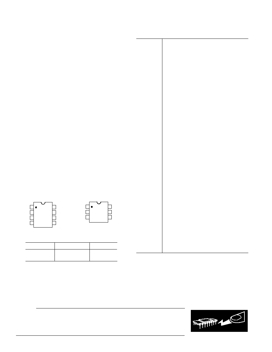
PIN CONFIGURATIONS
6-Lead SOT-23
(RT-6)
1
2
3
6
5
4
TOP VIEW
(Not to Scale)
ADG752
IN
D
VDD
S1
GND
S2
8-Lead
SOIC
(RM-8)
1
2
3
4
8
7
6
5
TOP VIEW
(Not to Scale)
NC = NO CONNECT
ADG752
NC
S1
D
VDD
S2
GND
IN
REV. A
相关PDF资料 |
PDF描述 |
|---|---|
| ADG212AKNZ | IC SWITCH QUAD SPST 16DIP |
| ADG211AKNZ | IC SWITCH QUAD SPST 16DIP |
| ADG211AKRZ-REEL7 | IC SWITCH QUAD SPST 16SOIC |
| ADG1436YCPZ-REEL7 | IC SWITCH DUAL SPDT 16LFCST |
| ADG1221BRMZ | IC SWITCH DUAL SPST 10MSOP |
相关代理商/技术参数 |
参数描述 |
|---|---|
| ADG752BRMZ | 制造商:Analog Devices 功能描述:IC, SWITCH, ANALOG, SINGLE, SPDT, SOIC- |
| ADG752BRMZ-REEL7 | 功能描述:IC VIDEO SWITCH SPDT 8MSOP RoHS:是 类别:集成电路 (IC) >> 接口 - 模拟开关,多路复用器,多路分解器 系列:- 标准包装:48 系列:- 功能:开关 电路:4 x SPST - NO 导通状态电阻:100 欧姆 电压电源:单/双电源 电压 - 电源,单路/双路(±):2 V ~ 12 V,±2 V ~ 6 V 电流 - 电源:50nA 工作温度:-40°C ~ 85°C 安装类型:表面贴装 封装/外壳:16-SOIC(0.154",3.90mm 宽) 供应商设备封装:16-SOIC 包装:管件 |
| ADG752BRT | 制造商:AD 制造商全称:Analog Devices 功能描述:CMOS, Low Voltage RF/Video, SPDT Switch |
| ADG752BRT-REEL | 功能描述:IC VIDEO SWITCH SPDT SOT23-6 RoHS:否 类别:集成电路 (IC) >> 接口 - 模拟开关,多路复用器,多路分解器 系列:- 标准包装:1,000 系列:- 功能:多路复用器 电路:1 x 4:1 导通状态电阻:- 电压电源:双电源 电压 - 电源,单路/双路(±):±5V 电流 - 电源:7mA 工作温度:-40°C ~ 85°C 安装类型:表面贴装 封装/外壳:16-SOIC(0.154",3.90mm 宽) 供应商设备封装:16-SOIC 包装:带卷 (TR) |
| ADG752BRT-REEL7 | 功能描述:IC VIDEO SWITCH SPDT SOT23-6 RoHS:否 类别:集成电路 (IC) >> 接口 - 模拟开关,多路复用器,多路分解器 系列:- 标准包装:1,000 系列:- 功能:多路复用器 电路:1 x 4:1 导通状态电阻:- 电压电源:双电源 电压 - 电源,单路/双路(±):±5V 电流 - 电源:7mA 工作温度:-40°C ~ 85°C 安装类型:表面贴装 封装/外壳:16-SOIC(0.154",3.90mm 宽) 供应商设备封装:16-SOIC 包装:带卷 (TR) |
发布紧急采购,3分钟左右您将得到回复。