- 您现在的位置:买卖IC网 > PDF目录22034 > ADM1021AARQZ-REEL (ON Semiconductor)IC SENSOR TEMP DUAL3/5.5V 16QSOP PDF资料下载
参数资料
| 型号: | ADM1021AARQZ-REEL |
| 厂商: | ON Semiconductor |
| 文件页数: | 11/16页 |
| 文件大小: | 0K |
| 描述: | IC SENSOR TEMP DUAL3/5.5V 16QSOP |
| 产品变化通告: | MFG CHG Notification ADI to ON Semi |
| 标准包装: | 2,500 |
| 功能: | 温度监控系统(传感器) |
| 传感器类型: | 内部和外部 |
| 感应温度: | 0°C ~ 100°C,外部传感器 |
| 精确度: | ±1°C 本地,±5°C 远程 |
| 拓扑: | ADC,比较器,多路复用器,寄存器库 |
| 输出类型: | SMBus? |
| 输出警报: | 是 |
| 输出风扇: | 无 |
| 电源电压: | 3 V ~ 5.5 V |
| 工作温度: | 0°C ~ 100°C |
| 安装类型: | 表面贴装 |
| 封装/外壳: | 16-SSOP(0.154",3.90mm 宽) |
| 供应商设备封装: | 16-QSOP |
| 包装: | 带卷 (TR) |
�� �
�
�ADM1021A�
�Table 11. DEVICE� ADDRESSES� (Note� 1)�
�ADD0� ADD1� Device� Address�
�0� 0� 0011� 000�
�low� period� of� the� clock� signal� and� remain� stable�
�during� the� high� period,� because� a� low-to-high�
�transition� when� the� clock� is� high� can� be� interpreted�
�as� a� stop� signal.� The� number� of� data� bytes� that� can�
�0�
�0�
�NC�
�NC�
�NC�
�1�
�NC�
�1�
�0�
�NC�
�1�
�0�
�0011� 001�
�0011� 010�
�0101� 001�
�0101� 010�
�0101� 011�
�1001� 100�
�be� transmitted� over� the� serial� bus� in� a� single� read�
�or� write� operation� is� limited� only� by� what� the�
�master� and� slave� devices� can� handle.�
�3.� When� all� data� bytes� have� been� read� or� written,�
�stop� conditions� are� established.� In� write� mode,� the�
�master� pulls� the� data� line� high� during� the� 10th�
�clock� pulse� to� assert� a� stop� condition.� In� read�
�1� NC� 1001� 101�
�1� 1� 1001� 110�
�1.� ADD0� and� ADD1� are� sampled� at� powerup� only.�
�The� serial� bus� protocol� operates� as� follows:�
�1.� The� master� initiates� data� transfer� by� establishing� a�
�start� condition,� defined� as� a� high-to-low� transition�
�on� the� serial� data� line� SDATA,� while� the� serial�
�clock� line� SCLK� remains� high.� This� indicates� that�
�an� address/data� stream� will� follow.� All� slave�
�peripherals� connected� to� the� serial� bus� respond� to�
�the� START� condition� and� shift� in� the� next� eight�
�bits,� consisting� of� a� 7-bit� address� (MSB� first)� plus�
�an� R/W� bit,� which� determines� the� direction� of� the�
�data� transfer,� that� is,� whether� data� will� be� written�
�to� or� read� from� the� slave� device.�
�The� peripheral� whose� address� corresponds� to� the�
�transmitted� address� responds� by� pulling� the� data�
�line� low� during� the� low� period� before� the� ninth�
�clock� pulse,� known� as� the� Acknowledge� Bit.� All�
�other� devices� on� the� bus� now� remain� idle� while� the�
�selected� device� waits� for� data� to� be� read� from� or�
�written� to� it.� If� the� R/W� bit� i� s� a� 0,� the� master� writes�
�to� the� slave� device.� If� the� R/W� bit� is� a� 1,� the�
�master� reads� from� the� slave� device.�
�2.� Data� is� sent� over� the� serial� bus� in� sequences� of�
�nine� clock� pulses,� eight� bits� of� data� followed� by� an�
�Acknowledge� Bit� from� the� slave� device.�
�Transitions� on� the� data� line� must� occur� during� the�
�mode,� the� master� device� overrides� the�
�acknowledge� bit� by� pulling� the� data� line� high�
�during� the� low� period� before� the� ninth� clock� pulse.�
�This� is� known� as� No� Acknowledge.� The� master�
�then� takes� the� data� line� low� during� the� low� period�
�before� the� 10th� clock� pulse,� then� high� during� the�
�10th� clock� pulse� to� assert� a� stop� condition.�
�Any� number� of� bytes� of� data� can� be� transferred� over� the�
�serial� bus� in� one� operation,� but� it� is� not� possible� to� mix� read�
�and� write� in� one� operation,� because� the� type� of� operation� is�
�determined� at� the� beginning� and� cannot� subsequently� be�
�changed� without� starting� a� new� operation.�
�For� the� ADM1021A,� write� operations� contain� either� one�
�or� two� bytes,� while� read� operations� contain� one� byte.�
�To� write� data� to� one� of� the� device� data� registers� or� read�
�data� from� it,� the� address� pointer� register� must� be� set� so� that�
�the� correct� data� register� is� addressed,� data� can� then� be� written�
�into� that� register� or� read� from� it.� The� first� byte� of� a� write�
�operation� always� contains� a� valid� address� that� is� stored� in� the�
�address� pointer� register.� If� data� is� to� be� written� to� the� device,�
�the� write� operation� contains� a� second� data� byte� that� is� written�
�to� the� register� selected� by� the� address� pointer� register.�
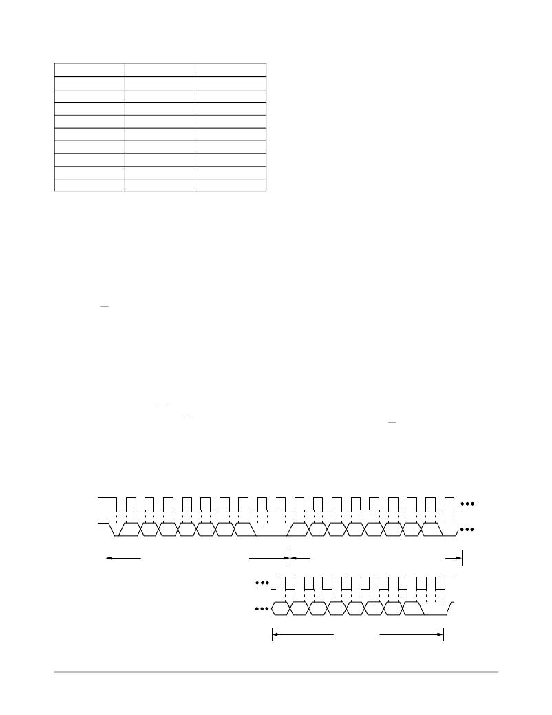
�This� is� illustrated� in� Figure� 14.� The� device� address� is� sent�
�over� the� bus� followed� by� R/W� set� to� 0.� This� is� followed� by�
�two� data� bytes.� The� first� data� byte� is� the� address� of� the�
�internal� data� register� to� be� written� to,� which� is� stored� in� the�
�address� pointer� register.� The� second� data� byte� is� the� data� to�
�be� written� to� the� internal� data� register.�
�1�
�9�
�1�
�9�
�SCLK�
�SDATA�
�A6�
�A5�
�A4�
�A3�
�A2�
�A1�
�A0�
�R/W�
�D7�
�D6�
�D5�
�D4�
�D3�
�D2�
�D1�
�D0�
�FRAME� 2�
�START� BY�
�MASTER�
�FRAME� 1�
�SERIAL� BUS� ADDRESS� BYTE�
�ACK.� BY�
�ADM1021A�
�1�
�ACK.� BY�
�ADM1021A�
�ADDRESS� POINTER� REGISTER� BYTE�
�9�
�SCLK� (CONTINUED)�
�SDATA� (CONTINUED)�
�D7�
�D6�
�D5�
�D4�
�D3�
�D2�
�D1�
�D0�
�FRAME� 3�
�DATA� BYTE�
�ACK.� BY� STOP� BY�
�ADM1021A� MASTER�
�Figure� 14.� Writing� a� Register� Address� to� the� Address� Pointer� Register,� then� Writing� Data� to� the� Selected� Register�
�http://onsemi.com�
�11�
�相关PDF资料 |
PDF描述 |
|---|---|
| EP1K10TC144-2N | IC ACEX 1K FPGA 10K 144-TQFP |
| ADM1021AARQZ | IC SENSOR TEMP DUAL3/5.5V 16QSOP |
| ADM1032ARM-REEL | IC TEMP MONITOR 85DEF 8MSOP |
| ADM1032ARM-1REEL7 | IC TEMP MONITOR 105DEF 8MSOP |
| ADT7463ARQ-REEL7 | IC SENSOR TEMP FAN-CTRL 24QSOP |
相关代理商/技术参数 |
参数描述 |
|---|---|
| ADM1021AARQZ-REEL7 | 功能描述:IC SENSOR TEMP DUAL3/5.5V 16QSOP RoHS:是 类别:集成电路 (IC) >> PMIC - 热管理 系列:- 标准包装:1 系列:- 功能:温度监控系统(传感器) 传感器类型:内部和外部 感应温度:-40°C ~ 125°C,外部传感器 精确度:±2.5°C 本地(最大值),±5°C 远程(最大值) 拓扑:ADC,比较器,寄存器库 输出类型:2 线 SMBus? 输出警报:无 输出风扇:无 电源电压:2.7 V ~ 5.5 V 工作温度:-40°C ~ 125°C 安装类型:表面贴装 封装/外壳:SOT-23-8 供应商设备封装:SOT-23-8 包装:Digi-Reel® 其它名称:296-22675-6 |
| ADM1021ARQ | 功能描述:IC SENSOR TEMP DUAL3/5.5V 16QSOP RoHS:否 类别:集成电路 (IC) >> PMIC - 热管理 系列:- 标准包装:1 系列:- 功能:温度监控系统(传感器) 传感器类型:内部和外部 感应温度:-40°C ~ 125°C,外部传感器 精确度:±2.5°C 本地(最大值),±5°C 远程(最大值) 拓扑:ADC,比较器,寄存器库 输出类型:2 线 SMBus? 输出警报:无 输出风扇:无 电源电压:2.7 V ~ 5.5 V 工作温度:-40°C ~ 125°C 安装类型:表面贴装 封装/外壳:SOT-23-8 供应商设备封装:SOT-23-8 包装:Digi-Reel® 其它名称:296-22675-6 |
| ADM1021ARQ-REEL | 功能描述:IC SENSOR TEMP DUAL3/5.5V 16QSOP RoHS:否 类别:集成电路 (IC) >> PMIC - 热管理 系列:- 标准包装:1 系列:- 功能:温度监控系统(传感器) 传感器类型:内部和外部 感应温度:-40°C ~ 125°C,外部传感器 精确度:±2.5°C 本地(最大值),±5°C 远程(最大值) 拓扑:ADC,比较器,寄存器库 输出类型:2 线 SMBus? 输出警报:无 输出风扇:无 电源电压:2.7 V ~ 5.5 V 工作温度:-40°C ~ 125°C 安装类型:表面贴装 封装/外壳:SOT-23-8 供应商设备封装:SOT-23-8 包装:Digi-Reel® 其它名称:296-22675-6 |
| ADM1021ARQREEL7 | 制造商:ANALOG DEVICES INC 功能描述: |
| ADM1021ARQ-REEL7 | 功能描述:IC SENSOR TEMP DUAL3/5.5V 16QSOP RoHS:否 类别:集成电路 (IC) >> PMIC - 热管理 系列:- 标准包装:1 系列:- 功能:温度监控系统(传感器) 传感器类型:内部和外部 感应温度:-40°C ~ 125°C,外部传感器 精确度:±2.5°C 本地(最大值),±5°C 远程(最大值) 拓扑:ADC,比较器,寄存器库 输出类型:2 线 SMBus? 输出警报:无 输出风扇:无 电源电压:2.7 V ~ 5.5 V 工作温度:-40°C ~ 125°C 安装类型:表面贴装 封装/外壳:SOT-23-8 供应商设备封装:SOT-23-8 包装:Digi-Reel® 其它名称:296-22675-6 |
发布紧急采购,3分钟左右您将得到回复。