- 您现在的位置:买卖IC网 > PDF目录373995 > ADM1052 (Analog Devices, Inc.) Precision Dual Voltage Regulator Controller PDF资料下载
参数资料
| 型号: | ADM1052 |
| 厂商: | Analog Devices, Inc. |
| 英文描述: | Precision Dual Voltage Regulator Controller |
| 中文描述: | 精密双稳压控制器 |
| 文件页数: | 3/8页 |
| 文件大小: | 164K |
| 代理商: | ADM1052 |
REV. A
ADM1052
–3–
ABSOLUTE MAXIMUM RATINGS
*
(T
A
= 25
°
C unless otherwise noted)
V
CC
to GND . . . . . . . . . . . . . . . . . . . . . . . . . . . . . . . . . . 14 V
SHDN1
,
SHDN2
to GND . . . . . . . . –0.3 V to (V
CC
+ 0.3 V)
SENSE1, SENSE2 to GND . . . . . . . . . . . . –0.3 V to +5.5 V
FORCE1, FORCE2 . . . . . . . . Short-Circuit to GND or V
CC
Continuous Power Dissipation (T
A
= 70
°
C) . . . . . . . 650 mW
8-Lead SOIC . . . . . . . . . . . . (Derate 8.3 mW/
°
C above 70
°
C)
Operating Temperature Range
Commercial (J Version) . . . . . . . . . . . . . . . . . . 0
°
C to 70
°
C
Storage Temperature Range . . . . . . . . . . . . –65
°
C to +150
°
C
Lead Temperature (Soldering, 10 sec) . . . . . . . . . . . . 300
°
C
*
This is a stress rating only and functional operation of the device at these or any
other conditions above those indicated in the operation sections of this specifica-
tion is not implied. Exposure to absolute maximum rating conditions for extended
periods of time may affect reliability.
THERMAL CHARACTERISTICS
8-Lead Small Outline Package:
JA
= 150
°
C/W
ORDERING GUIDE
Temperature
Range
0
°
C to 70
°
C
Package
Description
Package
Option
Model
ADM1052JR
8-Lead SOIC
SO-8
ADM1052
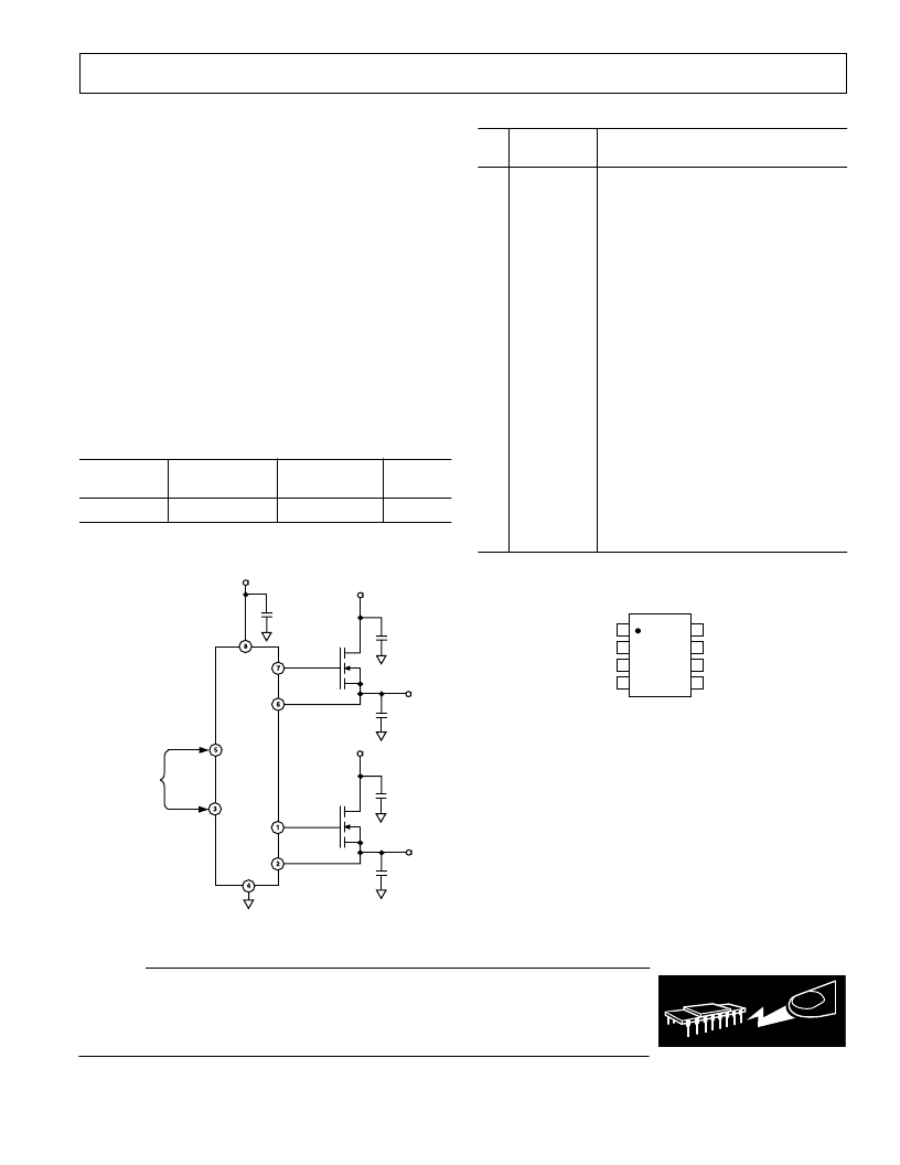
100 F
2
100 F
3.3V
V
OUT1
FORCE 1
SENSE 1
3.3V
V
OUT2
FORCE 2
SENSE 2
100 F
2 100 F
SHDN1
SHDN2
LEAVE OPEN OR
CONNECT TO
LOGIC SIGNALS
IF SHUTDOWN
REQUIRED
PHD55N03LT
MTD3055VL
1 F
12V
V
CC
GND
Figure 1. Test Circuit
PIN FUNCTION DESCRIPTIONS
Pin
No.
Mnemonic
Function
1
FORCE 2
Output of Channel 2 control amplifier to
gate of external N-channel MOSFET.
Input from source of external MOSFET to
inverting input of Channel 2 control
amplifier, via output voltage-setting feed-
back resistor network.
Digital Input. Active-low shutdown control
with 50
μ
A internal pull-up. The output
of Channel 2 control amplifier goes to
ground when
SHDN2
is taken low.
Device Ground Pin.
Digital Input. Active-low shutdown control
with 50
μ
A internal pull-up. The output
of Channel 1 control amplifier goes to
ground when
SHDN1
is taken low.
Input from source of external MOSFET
to inverting input of Channel 1 control
amplifier, via output voltage-setting
feedback resistor network.
Output of Channel 2 control amplifier to
gate of external N-channel MOSFET.
12 V Supply.
2
SENSE 2
3
SHDN2
4
5
GND
SHDN1
6
SENSE 1
7
FORCE 1
8
V
CC
PIN CONFIGURATION
TOP VIEW
(Not to Scale)
8
7
6
5
1
2
3
4
FORCE 2
SENSE 2
SHDN2
GND
V
CC
FORCE 1
SENSE 1
SHDN1
ADM1052
CAUTION
ESD (electrostatic discharge) sensitive device. Electrostatic charges as high as 4000 V readily
accumulate on the human body and test equipment and can discharge without detection. Although
the ADM1052 features proprietary ESD protection circuitry, permanent damage may occur on
devices subjected to high-energy electrostatic discharges. Therefore, proper ESD precautions are
recommended to avoid performance degradation or loss of functionality.
WARNING!
ESD SENSITIVE DEVICE
相关PDF资料 |
PDF描述 |
|---|---|
| ADM1052JR | Precision Dual Voltage Regulator Controller |
| ADM1060 | DIP Socket; No. of Contacts:56; Pitch Spacing:0.07"; Row Spacing:0.6"; Terminal Type:PC Board; Leaded Process Compatible:Yes; Peak Reflow Compatible (260 C):No RoHS Compliant: Yes |
| ADM1060ARU | CON-HDR64POS2ROW 4WALL.1X.1SP,RTANG,LOPF |
| ADM1064 | Super Sequencer with Voltage Readback ADC |
| ADM1064ACP | Super Sequencer with Voltage Readback ADC |
相关代理商/技术参数 |
参数描述 |
|---|---|
| ADM1052JR | 制造商:Analog Devices 功能描述:DC DC Cntrlr Dual-OUT Prog Sw 3.3V Input 8-Pin SOIC 制造商:Rochester Electronics LLC 功能描述:DUAL BUS TERMINATOR - Bulk |
| ADM1052JR-REEL | 制造商:Analog Devices 功能描述:DC DC Cntrlr Dual-OUT Prog Sw 3.3V Input 8-Pin SOIC T/R 制造商:Rochester Electronics LLC 功能描述:DUAL BUS TERMINATOR - Tape and Reel |
| ADM1052JR-REEL7 | 制造商:Analog Devices 功能描述:DC DC Cntrlr Dual-OUT Prog Sw 3.3V Input 8-Pin SOIC T/R |
| ADM1060 | 制造商:AD 制造商全称:Analog Devices 功能描述:Communications System Supervisory/Sequencing Circuit |
| ADM1060ARU | 功能描述:IC SUPERVIS/SEQUENC 7-CH 28TSSOP RoHS:否 类别:集成电路 (IC) >> PMIC - 监控器 系列:Super Sequencer® 标准包装:1 系列:- 类型:简单复位/加电复位 监视电压数目:1 输出:开路漏极或开路集电极 复位:高有效 复位超时:- 电压 - 阀值:1.8V 工作温度:-40°C ~ 125°C 安装类型:表面贴装 封装/外壳:6-TSOP(0.059",1.50mm 宽)5 引线 供应商设备封装:5-TSOP 包装:剪切带 (CT) 其它名称:NCP301HSN18T1GOSCT |
发布紧急采购,3分钟左右您将得到回复。