- 您现在的位置:买卖IC网 > PDF目录373996 > ADM1066ASU-U3 (ANALOG DEVICES INC) Multisupply Supervisor/Sequencer with Margining Control and Auxiliary ADC Inputs PDF资料下载
参数资料
| 型号: | ADM1066ASU-U3 |
| 厂商: | ANALOG DEVICES INC |
| 元件分类: | 电源管理 |
| 英文描述: | Multisupply Supervisor/Sequencer with Margining Control and Auxiliary ADC Inputs |
| 中文描述: | 2-CHANNEL POWER SUPPLY SUPPORT CKT, PQFP48 |
| 封装: | 7 X 7 MM, MO-026ABC, TQFP-48 |
| 文件页数: | 12/32页 |
| 文件大小: | 861K |
| 代理商: | ADM1066ASU-U3 |
第1页第2页第3页第4页第5页第6页第7页第8页第9页第10页第11页当前第12页第13页第14页第15页第16页第17页第18页第19页第20页第21页第22页第23页第24页第25页第26页第27页第28页第29页第30页第31页第32页
ADM1066
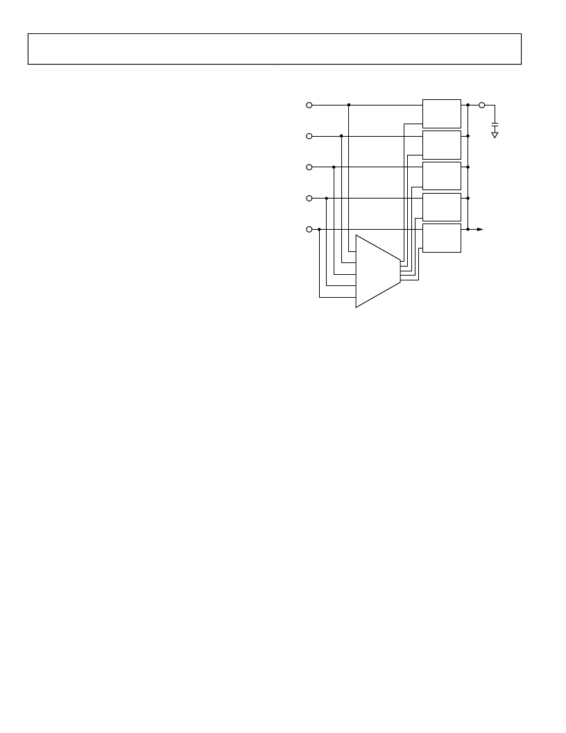
POWERING THE ADM1066
The ADM1066 is powered from the highest voltage input on
either the positive-only supply inputs (VPn) or the high voltage
supply input (VH). This technique offers improved redundancy
as the device is not dependent on any particular voltage rail to
keep it operational. The same pins are used for supply fault
detection (discussed later in the next section). A VDD arbitrator
on the device chooses which supply to use. The arbitrator can
be considered an OR’ing of five LDOs together. A supply
comparator chooses which of the inputs is highest and selects
this one to provide the on-chip supply. There is minimal
switching loss with this architecture (~0.2 V), resulting in the
ability to power the ADM1066 from a supply as low as 3.0 V.
Note that the supply on the VXn pins cannot be used to power
the device.
Rev. 0 | Page 12 of 32
An external capacitor to GND is required to decouple the on-
chip supply from noise. This capacitor should be connected to
the VDDCAP pin, as shown in Figure 21. The capacitor has
another use during brownouts (momentary loss of power).
Under these conditions, when the input supply (VPn or VH)
dips transiently below V
DD
, the synchronous rectifier switch
immediately turns off so that it does not pull V
DD
down. The
V
DD
cap can then act as a reservoir to keep the device active
until the next highest supply takes over the powering of the
device. 10 μF is recommended for this reservoir/decoupling
function.
Note that when two or more supplies are within 100 mV of each
other, the supply that takes control of V
DD
first keeps control.
For example, if VP1 is connected to a 3.3 V supply, then V
DD
powers up to approximately 3.1 V through VP1. If VP2 is then
connected to another 3.3 V supply, VP1 still powers the device,
unless VP2 goes 100 mV higher than VP1.
SUPPLY
COMPARATOR
IN
EN
OUT
4.75V
LDO
IN
EN
OUT
4.75V
LDO
IN
EN
OUT
4.75V
LDO
IN
EN
OUT
4.75V
LDO
IN
EN
OUT
4.75V
LDO
VH
VP4
VP3
VP2
VP1
VDDCAP
INTERNAL
DEVICE
SUPPLY
0
Figure 21. VDD Arbitrator Operation
相关PDF资料 |
PDF描述 |
|---|---|
| ADM1066ACP | Multisupply Supervisor/Sequencer with Margining Control and Auxiliary ADC Inputs |
| ADM1066ACP-REEL | Multisupply Supervisor/Sequencer with Margining Control and Auxiliary ADC Inputs |
| ADM1066ACP-REEL7 | Multisupply Supervisor/Sequencer with Margining Control and Auxiliary ADC Inputs |
| ADM1066ACP-U3 | Multisupply Supervisor/Sequencer with Margining Control and Auxiliary ADC Inputs |
| ADM1066 | Multisupply Supervisor/Sequencer with Margining Control and Auxiliary ADC Inputs |
相关代理商/技术参数 |
参数描述 |
|---|---|
| ADM1066ASUZ | 功能描述:IC SUPERVISOR/SEQUENCER 48-TQFP RoHS:是 类别:集成电路 (IC) >> PMIC - 监控器 系列:Super Sequencer® 其它有关文件:STM6905 View All Specifications 标准包装:1 系列:- 类型:多压监控器 监视电压数目:5 输出:开路漏极或开路集电极 复位:低有效 复位超时:最小为 140 ms 电压 - 阀值:2.188V,2.955V,可调,可调,可调 工作温度:-40°C ~ 85°C 安装类型:表面贴装 封装/外壳:8-TSSOP,8-MSOP(0.118",3.00mm 宽) 供应商设备封装:8-TSSOP 包装:Digi-Reel® 产品目录页面:1197 (CN2011-ZH PDF) 其它名称:497-8728-6 |
| ADM1066ASUZ-REEL | 功能描述:IC SEQUENCER/SUPERVISOR 48TQFP RoHS:是 类别:集成电路 (IC) >> PMIC - 监控器 系列:Super Sequencer® 标准包装:1 系列:- 类型:简单复位/加电复位 监视电压数目:1 输出:开路漏极或开路集电极 复位:高有效 复位超时:- 电压 - 阀值:1.8V 工作温度:-40°C ~ 125°C 安装类型:表面贴装 封装/外壳:6-TSOP(0.059",1.50mm 宽)5 引线 供应商设备封装:5-TSOP 包装:剪切带 (CT) 其它名称:NCP301HSN18T1GOSCT |
| ADM1066ASUZ-REEL7 | 功能描述:IC SEQUENCER/SUPERVISOR 48TQFP RoHS:是 类别:集成电路 (IC) >> PMIC - 监控器 系列:Super Sequencer® 标准包装:1 系列:- 类型:简单复位/加电复位 监视电压数目:1 输出:开路漏极或开路集电极 复位:高有效 复位超时:- 电压 - 阀值:1.8V 工作温度:-40°C ~ 125°C 安装类型:表面贴装 封装/外壳:6-TSOP(0.059",1.50mm 宽)5 引线 供应商设备封装:5-TSOP 包装:剪切带 (CT) 其它名称:NCP301HSN18T1GOSCT |
| ADM1067 | 制造商:AD 制造商全称:Analog Devices 功能描述:Super Sequencer with Open-Loop Margining DACs |
| ADM1067ACP | 制造商:Analog Devices 功能描述:Sequencer 40-Pin LFCSP EP |
发布紧急采购,3分钟左右您将得到回复。