- 您现在的位置:买卖IC网 > PDF目录373996 > ADM1185_07 (Analog Devices, Inc.) Quad Voltage Monitor and Sequencer PDF资料下载
参数资料
| 型号: | ADM1185_07 |
| 厂商: | Analog Devices, Inc. |
| 英文描述: | Quad Voltage Monitor and Sequencer |
| 中文描述: | 四电压监视和时序 |
| 文件页数: | 9/16页 |
| 文件大小: | 270K |
| 代理商: | ADM1185_07 |
ADM1185
THEORY OF OPERATION
The operation of the ADM1185 is explained in this section in
the context of the device in a voltage monitoring and sequencing
application (see Figure 18). In this application, the ADM1185
monitors four separate voltage rails, turns on three regulators in
a predefined sequence, and generates a power-good signal to
turn on a controller when all power supplies are up and stable.
POWER-ON SEQUENCING AND MONITORING
The main supply, in this case 3.3 V, powers up the device via the
VCC pin as the voltage rises. A supply voltage of 2.7 V to 5.5 V
is needed to power the device.
The VIN1 pin monitors the main 3.3 V supply. An external
resistor divider scales this voltage down for monitoring at the
VIN1 pin. The resistor ratio is chosen so that the VIN1 voltage
is 0.6 V when the main voltage rises to the preferred level at start-
up (a voltage below the nominal 3.3 V level). R1 is 4.6 kΩ and
R2 is 1.2 kΩ, so a voltage level of 2.9 V corresponds to 0.6 V on
the noninverting input of the first comparator (see Figure 17).
Rev. 0 | Page 9 of 16
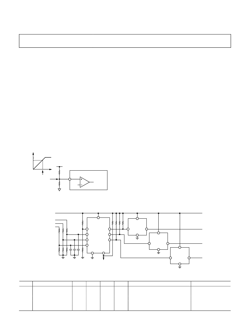
VIN1
1.2k
4.6k
0.6V
TO LOGIC
CORE
ADM1185
3.3V
2.9V
0V
V
t
2.9V SUPPLY
GIVES 0.6V
AT VIN1 PIN
0
Figure 17. Setting the Undervoltage Threshold with an
External Resistor Divider
OUT1 is an open-drain active high output. In this application,
OUT1 is connected to the enable pin of a regulator. Before the
voltage on VIN1 has reached 0.6 V, this output is switched to
ground, disabling Regulator 1. Note that all outputs are driven
to ground as long as there is 1 V on the VCC pin of the ADM1185.
When the main system voltage reaches 2.9 V, VIN1 detects 0.6 V.
This causes OUT1 to assert after a 190 ms (typical) delay. When
this occurs, the open-drain output switches high, and the external
pull-up resistor pulls the voltage on the Regulator 1 enable pin
above its turn-on threshold, turning on the output of Regulator 1.
The assertion of OUT1 turns on Regulator 1. The 2.5 V output
of this regulator begins to rise. This is detected by input VIN2
(with a similar resistor divider scheme as shown in Figure 18).
When VIN2 detects the 2.5 V rail rising above its UV point, it
asserts output OUT2, which turns on Regulator 2. A capacitor
can be placed on the VIN2 pin to slow the rise of the voltage on
this pin. This effectively sets a time delay between the 2.5 V rail
powering up and the next enabled regulator.
The same scheme is implemented with the other input and
output pins. Every rail that is turned on via an output pin,
OUTx, is monitored via an input pin VIN(x+1).
The final comparator inside the VIN4 pin detects the final supply
turning on, which is 1.2 V in this case. The output pins, OUT1
to OUT3 are logically AND’ed together to generate a system
power-good signal (PWRGD). There is an internal 190 ms delay
(typical) associated with the assertion of the PWRGD output.
Table 5 is a truth table that steps through the power-on sequence of
the outputs. Any associated internal time delays are also shown.
2.5V OUT
1.8V OUT
1.2V OUT
3.3V IN
2.5V OUT
1.8V OUT
1.2V OUT
OUT1
VIN1
OUT2
VIN2
OUT3
VIN3
VIN4
GND
PWRGD
POWER
GOOD
VCC
ADM1185
GND
REGULATOR1
IN
EN
OUT
GND
REGULATOR2
IN
EN
OUT
GND
REGULATOR3
IN
EN
OUT
0
Figure 18. Voltage Monitoring and Sequencing Application Diagram
Table 5. Truth Table
State
State Name
1
Reset
2
OUT1 On
3
OUT1, OUT2 On
4
OUT1, OUT2, OUT3 On
5
Power Good
OUT1
0
1
1
1
1
OUT2
0
0
1
1
1
OUT3
0
0
0
1
1
OUT4
0
0
0
0
1
Next Event
VIN1 high for 190 ms
VIN1 and VIN2 high for 30 μs
VIN1 and VIN3 high for 30 μs
All high for 190 ms
VIN2 , VIN3, or VIN4 low for 30 μs
Next State
OUT1 On
OUT1, OUT2 On
OUT1, OUT2, OUT3 On
Power Good
OUT1, OUT2, OUT3 On
相关PDF资料 |
PDF描述 |
|---|---|
| ADM1185ARMZ-1REEL7 | Quad Voltage Monitor and Sequencer |
| ADM1232A | Microprocessor Supervisory Circuit |
| ADM1232 | Microprocessor Supervisory Circuit |
| ADM1232AN | Microprocessor Supervisory Circuit |
| ADM1232ARM | Microprocessor Supervisory Circuit |
相关代理商/技术参数 |
参数描述 |
|---|---|
| ADM1185ARMZ | 制造商:AD 制造商全称:Analog Devices 功能描述:Quad Voltage Monitor and Sequencer |
| ADM1185ARMZ-1 | 制造商:Analog Devices 功能描述:VOLT SUPERVISOR MONITOR 10MSOP - Rail/Tube 制造商:Analog Devices 功能描述:VOLT MONITOR QUAD + SEQ SMD 1185 |
| ADM1185ARMZ-1REEL7 | 功能描述:IC VOLT MONITOR/SEQUENCER 10MSOP RoHS:是 类别:集成电路 (IC) >> PMIC - 监控器 系列:- 标准包装:100 系列:- 类型:简单复位/加电复位 监视电压数目:1 输出:开路漏极,开路漏极 复位:高有效/低有效 复位超时:最小为 250 ms 电压 - 阀值:4.37V,4.62V 工作温度:0°C ~ 70°C 安装类型:表面贴装 封装/外壳:8-SOIC(0.154",3.90mm 宽) 供应商设备封装:8-SOIC 包装:管件 产品目录页面:1337 (CN2011-ZH PDF) |
| ADM1186 | 制造商:AD 制造商全称:Analog Devices 功能描述:Quad Voltage Up and Down Sequencer and Monitor with Programmable Timing |
| ADM1186-1ARQZ | 功能描述:IC SEQUENCER/MONITOR QUAD 20QSOP RoHS:是 类别:集成电路 (IC) >> PMIC - 监控器 系列:- 其它有关文件:STM6905 View All Specifications 标准包装:1 系列:- 类型:多压监控器 监视电压数目:5 输出:开路漏极或开路集电极 复位:低有效 复位超时:最小为 140 ms 电压 - 阀值:2.188V,2.955V,可调,可调,可调 工作温度:-40°C ~ 85°C 安装类型:表面贴装 封装/外壳:8-TSSOP,8-MSOP(0.118",3.00mm 宽) 供应商设备封装:8-TSSOP 包装:Digi-Reel® 产品目录页面:1197 (CN2011-ZH PDF) 其它名称:497-8728-6 |
发布紧急采购,3分钟左右您将得到回复。