- 您现在的位置:买卖IC网 > PDF目录22107 > ADM1275-3ACPZ (Analog Devices Inc)IC HOT SWAP CTRL PMBUS 20LFCSP PDF资料下载
参数资料
| 型号: | ADM1275-3ACPZ |
| 厂商: | Analog Devices Inc |
| 文件页数: | 12/48页 |
| 文件大小: | 0K |
| 描述: | IC HOT SWAP CTRL PMBUS 20LFCSP |
| 标准包装: | 1 |
| 类型: | 热交换控制器 |
| 应用: | 通用 |
| 内部开关: | 无 |
| 电流限制: | 可调 |
| 电源电压: | 2.95 V ~ 20 V |
| 工作温度: | -40°C ~ 85°C |
| 安装类型: | 表面贴装 |
| 封装/外壳: | 20-WQFN 裸露焊盘,CSP |
| 供应商设备封装: | 20-LFCSP-WQ(5x5) |
| 包装: | 托盘 |
| 配用: | EVAL-ADM1275EBZ-ND - BOARD EVALUATION FOR ADM1275 |
第1页第2页第3页第4页第5页第6页第7页第8页第9页第10页第11页当前第12页第13页第14页第15页第16页第17页第18页第19页第20页第21页第22页第23页第24页第25页第26页第27页第28页第29页第30页第31页第32页第33页第34页第35页第36页第37页第38页第39页第40页第41页第42页第43页第44页第45页第46页第47页第48页
�� �
�
�ADM1275�
�Data� Sheet�
�VCC�
�UV�
�OV�
�1�
�2�
�3�
�20�
�19�
�18�
�SENSE+�
�SENSE–�
�GATE�
�VCAP�
�ISET�
�SS�
�TIMER�
�4�
�5�
�6�
�7�
�ADM1275-3�
�TOP� VIEW�
�(Not� to� Scale)�
�17�
�16�
�15�
�14�
�GND�
�VOUT�
�FLB�
�PWRGD�
�OV�
�VCAP�
�ISET�
�SS�
�TIMER�
�1�
�2�
�3�
�4�
�5�
�PIN� 1�
�INDICATOR�
�ADM1275-3�
�TOP� VIEW�
�(Not� to� Scale)�
�15� GND�
�14� VOUT�
�13� FLB�
�12� PWRGD�
�11� SCL�
�LATCH� 8�
�13�
�SCL�
�ADR�
�9�
�12�
�SDA�
�ENABLE� 10�
�11�
�GPO2/ALERT2�
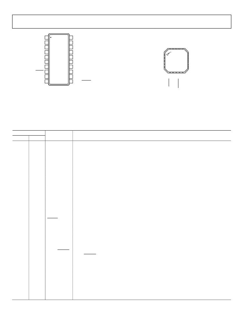
�Figure� 6.� ADM1275� -3� Pin� Configuration,� QSOP�
�NOTES�
�1.� SOLDER� THE� EXPOSED� PADDLE� TO�
�THE� BOARD� TO� IMPROVE� THERMAL�
�DISSIPATION.� THE� EXPOSED� PADDLE�
�CAN� BE� CONNECTED� TO� GROUND.�
�Figure� 7.� ADM1275� -3� Pin� Configuration,� LFCSP�
�Table� 7.� ADM1275� -3� Pin� Function� Descriptions�
�Pin� No.�
�QSOP� LFCSP�
�1� 19�
�Mnemonic�
�VCC�
�Description�
�Positive� Supply� Input� Pin.� An� undervoltage� lockout� (UVLO)� circuit� resets� the� device� when� a� low�
�supply� voltage� is� detected.� GATE� is� held� low� when� the� supply� is� below� UVLO.� During� normal�
�operation,� this� pin� should� remain� greater� than� or� equal� to� SENSE+� to� ensure� that� specifications� are�
�adhered� to.� No� sequencing� is� required.�
�2�
�20�
�UV�
�Undervoltage� Input� Pin.� An� external� resistor� divider� is� used� from� the� supply� to� this� pin� to� allow� an�
�internal� comparator� to� detect� whether� the� supply� is� under� the� UV� limit.�
�3�
�1�
�OV�
�Overvoltage� Input� Pin.� An� external� resistor� divider� is� used� from� the� supply� to� this� pin� to� allow� an�
�internal� comparator� to� detect� whether� the� supply� is� above� the� OV� limit.�
�4�
�2�
�VCAP�
�Internal� Regulated� Supply.� A� capacitor� with� a� value� of� 1� μF� or� greater� should� be� placed� on� this� pin�
�to� maintain� good� accuracy.� This� pin� can� be� used� as� a� reference� to� program� the� ISET� pin� voltage.�
�5�
�3�
�ISET�
�This� pin� allows� the� current� limit� threshold� to� be� programmed.� The� default� limit� is� set� when� this� pin�
�is� connected� directly� to� VCAP.� To� achieve� a� user-defined� sense� voltage,� the� current� limit� can� be�
�adjusted� using� a� resistor� divider� from� VCAP.� An� external� reference� can� also� be� used.�
�6�
�4�
�SS�
�Soft� Start� Pin.� A� capacitor� is� used� on� this� pin� to� set� the� soft� start� ramp� profile.� The� voltage� on� the�
�SS� pin� controls� the� current� sense� voltage� limit,� which� controls� the� inrush� current� profile.�
�7�
�5�
�TIMER�
�Timer� Pin.� An� external� capacitor,� C� TIMER� ,� sets� an� initial� timing� cycle� delay� and� a� fault� delay.� The� GATE�
�pin� is� pulled� low� when� the� voltage� on� the� TIMER� pin� exceeds� the� upper� threshold.�
�8�
�6�
�LATCH�
�Signals� that� the� device� is� latching� off� after� an� overcurrent� fault.� The� device� can� be� configured� for�
�automatic� retry� after� latch-off� by� connecting� this� pin� directly� back� to� the� UV� pin.�
�9�
�7�
�ADR�
�PMBus� Address� Pin.� This� pin� can� be� tied� to� GND,� tied� to� VCAP,� left� floating,� or� tied� low� through� a�
�resistor� to� set� four� different� PMBus� addresses� (see� the� Device� Addressing� section).�
�10�
�8�
�ENABLE�
�Digital� Logic� Input.� This� input� must� be� high� to� allow� the� ADM1275� -3� hot-swap� controller� to� begin� a�
�power-up� sequence.� If� this� pin� is� held� low,� the� ADM1275� -3� is� prevented� from� powering� up.� There� is�
�no� internal� pull-up� on� this� pin.�
�11�
�9�
�GPO2/ALERT2�
�General-Purpose� Digital� Output� (GPO2).�
�Alert� (ALERT2).� This� pin� can� be� configured� to� generate� an� alert� signal� when� one� or� more� fault� or�
�warning� conditions� are� detected.�
�At� power-up,� this� pin� indicates� the� FET� health� mode� by� default.� There� is� no� internal� pull-up� on� this� pin.�
�12�
�13�
�14�
�10�
�11�
�12�
�SDA�
�SCL�
�PWRGD�
�Serial� Data� Input/Output� Pin.� Open-drain� input/output.� Requires� an� external� resistive� pull-up.�
�Serial� Clock� Pin.� Open-drain� input.� Requires� an� external� resistive� pull-up.�
�Power-Good� Signal.� Used� to� indicate� that� the� supply� is� within� tolerance.� This� signal� is� based� on� the�
�voltage� present� on� the� FLB� pin.�
�15�
�13�
�FLB�
�Foldback� Pin.� A� foldback� resistor� divider� is� placed� from� the� source� of� the� FET� to� this� pin.� Foldback� is�
�used� to� reduce� the� current� limit� when� the� source� voltage� drops.� The� foldback� feature� ensures� that�
�the� power� through� the� FET� is� not� increased� beyond� the� SOA� limits.�
�Rev.� D� |� Page� 12� of� 48�
�相关PDF资料 |
PDF描述 |
|---|---|
| VI-234-EV-F2 | CONVERTER MOD DC/DC 48V 150W |
| TAP104M035CCS | CAP TANT 0.1UF 35V 20% RADIAL |
| VI-234-EV-F1 | CONVERTER MOD DC/DC 48V 150W |
| TAP104M035BRW | CAP TANT 0.1UF 35V 20% RADIAL |
| VI-233-EV-F4 | CONVERTER MOD DC/DC 24V 150W |
相关代理商/技术参数 |
参数描述 |
|---|---|
| ADM1275-3ACPZ-R7 | 功能描述:IC HOT SWAP CTRL PMBUS 20LFCSP RoHS:是 类别:集成电路 (IC) >> PMIC - 热交换 系列:- 产品培训模块:Lead (SnPb) Finish for COTS Obsolescence Mitigation Program 标准包装:119 系列:- 类型:热交换控制器 应用:通用型,PCI Express? 内部开关:无 电流限制:- 电源电压:3.3V,12V 工作温度:-40°C ~ 85°C 安装类型:表面贴装 封装/外壳:80-TQFP 供应商设备封装:80-TQFP(12x12) 包装:托盘 产品目录页面:1423 (CN2011-ZH PDF) |
| ADM1275-3ARQZ | 功能描述:IC HOT SWAP CTRL PMBUS 20QSOP RoHS:是 类别:集成电路 (IC) >> PMIC - 热交换 系列:- 标准包装:50 系列:- 类型:热交换控制器 应用:-48V 远程电力系统,AdvancedTCA ? 系统,高可用性 内部开关:无 电流限制:可调 电源电压:11.5 V ~ 14.5 V 工作温度:-40°C ~ 85°C 安装类型:表面贴装 封装/外壳:10-TFSOP,10-MSOP(0.118",3.00mm 宽) 供应商设备封装:10-MSOP 包装:管件 |
| ADM1275-3ARQZ-R7 | 功能描述:IC HOT SWAP CTRL PMBUS 20QSOP RoHS:是 类别:集成电路 (IC) >> PMIC - 热交换 系列:- 产品培训模块:Lead (SnPb) Finish for COTS Obsolescence Mitigation Program 标准包装:119 系列:- 类型:热交换控制器 应用:通用型,PCI Express? 内部开关:无 电流限制:- 电源电压:3.3V,12V 工作温度:-40°C ~ 85°C 安装类型:表面贴装 封装/外壳:80-TQFP 供应商设备封装:80-TQFP(12x12) 包装:托盘 产品目录页面:1423 (CN2011-ZH PDF) |
| ADM1276 | 制造商:AD 制造商全称:Analog Devices 功能描述:Hot Swap Controller and Digital Power and Energy Monitoring with PMBus Interface |
| ADM1276-3ACPZ | 功能描述:IC HOT SWAP CTRLR PMBUS 20LFCSP RoHS:是 类别:集成电路 (IC) >> PMIC - 热交换 系列:- 产品培训模块:Lead (SnPb) Finish for COTS Obsolescence Mitigation Program 标准包装:119 系列:- 类型:热交换控制器 应用:通用型,PCI Express? 内部开关:无 电流限制:- 电源电压:3.3V,12V 工作温度:-40°C ~ 85°C 安装类型:表面贴装 封装/外壳:80-TQFP 供应商设备封装:80-TQFP(12x12) 包装:托盘 产品目录页面:1423 (CN2011-ZH PDF) |
发布紧急采购,3分钟左右您将得到回复。