- 您现在的位置:买卖IC网 > PDF目录10181 > ADM208EARUZ-REEL (Analog Devices Inc)IC TXRX RS-232 5V 0.1UF 24TSSOP PDF资料下载
参数资料
| 型号: | ADM208EARUZ-REEL |
| 厂商: | Analog Devices Inc |
| 文件页数: | 2/20页 |
| 文件大小: | 0K |
| 描述: | IC TXRX RS-232 5V 0.1UF 24TSSOP |
| 标准包装: | 2,500 |
| 类型: | 收发器 |
| 驱动器/接收器数: | 4/4 |
| 规程: | RS232 |
| 电源电压: | 4.5 V ~ 5.5 V |
| 安装类型: | 表面贴装 |
| 封装/外壳: | 24-TSSOP(0.173",4.40mm 宽) |
| 供应商设备封装: | 24-TSSOP |
| 包装: | 带卷 (TR) |
ADM206E/ADM207E/ADM208E/ADM211E/ADM213E
Rev. E | Page 10 of 20
THEORY OF OPERATION
The ADM206E/ADM207E/ADM208E/ADM211E/ADM213E
are ruggedized RS-232 line drivers/receivers that operate from a
single 5 V supply. Step-up voltage converters coupled with level
shifting transmitters and receivers allow RS-232 levels to be
developed while operating from a single 5 V supply.
Features include low power consumption, high transmission
rates, and compliance with the EU directive on EMC, which
includes protection against radiated and conducted interfere-
ence, including high levels of electrostatic discharge.
All RS-232 inputs and outputs contain protection against
electrostatic discharges up to ±15 kV and electrical fast tran-
sients up to ±2 kV. This ensures compliance to IEC 100042
and IEC 100044 requirements.
The devices are ideally suited for operation in electrically harsh
environments or where RS-232 cables are plugged/unplugged
frequently. They are also immune to high RF field strengths
without special shielding precautions.
Emissions are also controlled to within very strict limits.
TTL/CMOS technology is used to keep the power dissipation to
an absolute minimum, allowing maximum battery life in
portable applications. The ADM2xxE is a modification,
enhancement, and improvement to the ADM2xx family and its
derivatives. It is essentially plug-in compatible and does not
have materially different applications.
CIRCUIT DESCRIPTION
The internal circuitry consists of four main sections:
A charge pump voltage converter.
5 V logic to EIA-232 transmitters.
EIA-232 to 5 V logic receivers.
Transient protection circuit on all I/O lines.
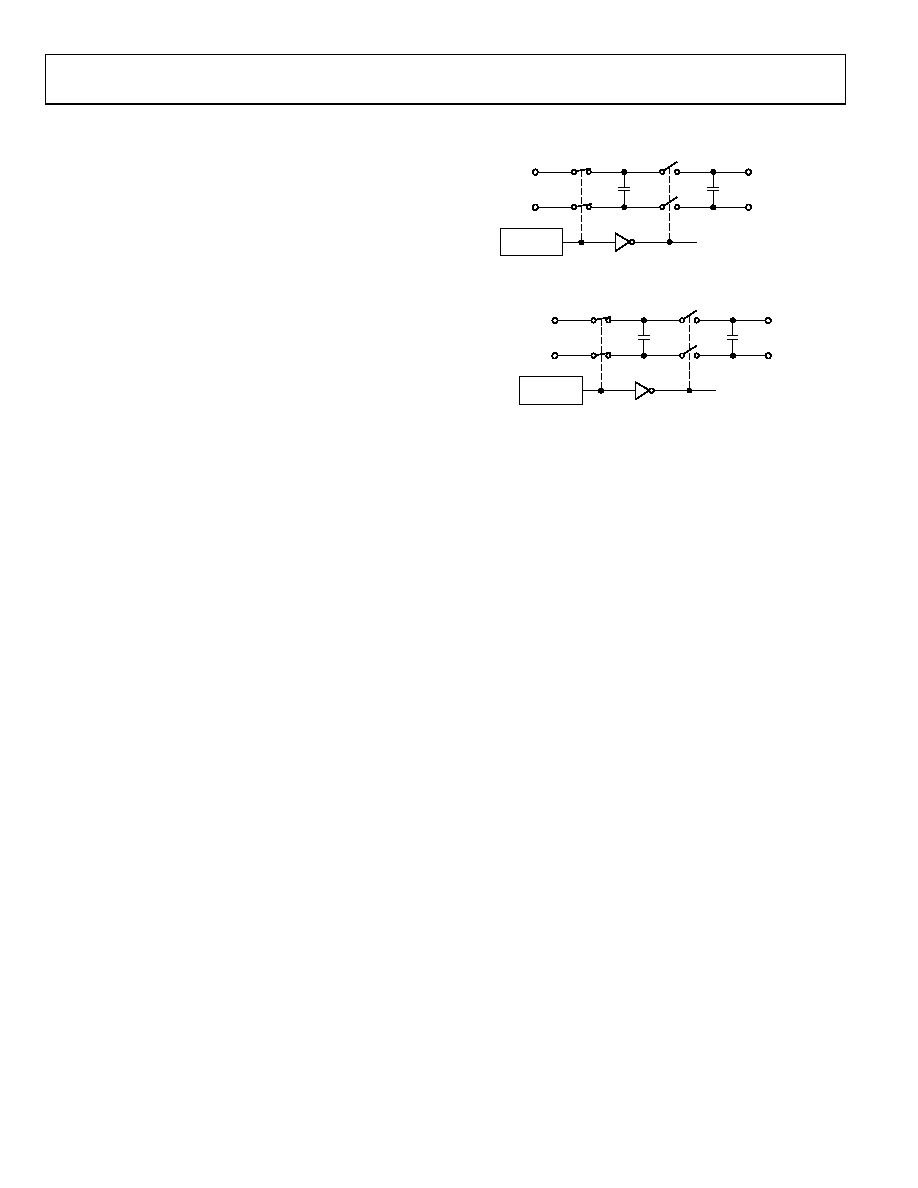
Charge Pump DC-to-DC Voltage Converter
The charge pump voltage converter consists of a 200 kHz
oscillator and a switching matrix. The converter generates a
±10 V supply from the input 5 V level. This is done in two
stages using a switched capacitor technique as illustrated in
Figure 20 and Figure 21. First, the 5 V input supply is doubled
to 10 V using Capacitor C1 as the charge storage element. The
10 V level is then inverted to generate 10 V using C2 as the
storage element.
Capacitor C3 and Capacitor C4 are used to reduce the output
ripple. If desired, larger capacitors (up to 47 μF) can be used for
Capacitor C1 to Capacitor C4. This facilitates direct substitution
with older generation charge pump RS-232 transceivers.
The V+ and V– supplies can also be used to power external
circuitry, if the current requirements are small (see the Typical
+
VCC
GND
S1
S2
C1
S3
S4
C3
V+ = 2VCC
VCC
INTERNAL
OSCILLATOR
00
06
8-
020
Figure 20. Charge Pump Voltage Doubler
FROM
VOLTAGE
DOUBLER
+
V+
GND
S1
S2
C2
S3
S4
C4
GND
V– = –(V+)
INTERNAL
OSCILLATOR
00
06
8-
021
Figure 21. Charge Pump Voltage Inverter
Transmitter (Driver) Section
The drivers convert 5 V logic input levels into EIA-232 output
levels. With VCC = 5 V and driving an EIA-232 load, the output
voltage swing is typically ±9 V.
Unused inputs can be left unconnected, as an internal 400 kΩ
pull-up resistor pulls them high, forcing the outputs into a low
state. The input pull-up resistors typically source 8 μA when
grounded, so unused inputs should either be connected to VCC
or left unconnected in order to minimize power consumption.
Receiver Section
The receivers are inverting level shifters that accept EIA-232 input
levels and translate them into 5 V logic output levels. The inputs
have internal 5 kΩ pull-down resistors to ground and are
protected against overvoltages of up to ±25 V. The guaranteed
switching thresholds are 0.4 V minimum and 2.4 V maximum.
Unconnected inputs are pulled to 0 V by the internal 5 kΩ pull-
down resistor. This, therefore, results in a Logic 1 output level for
unconnected inputs or for inputs connected to GND.
The receivers have Schmitt trigger inputs with a hysteresis level
of 0.65 V. This ensures error-free reception for both noisy
inputs and for inputs with slow transition times.
ENABLE AND SHUTDOWN
Table 3 and Table 4 are truth tables for the enable and shutdown
control signals. The enable function is intended to facilitate data
bus connections where it is desirable to tristate the receiver
outputs. In the disabled mode, all receiver outputs are placed in
a high impedance state. The shutdown function is intended to
shut down the device, thereby minimizing the quiescent
current. In shutdown, all transmitters are disabled and all
receivers on the ADM211E are tristated.
相关PDF资料 |
PDF描述 |
|---|---|
| VE-B3R-MW-F2 | CONVERTER MOD DC/DC 7.5V 100W |
| VE-25H-CU-F1 | CONVERTER MOD DC/DC 52V 200W |
| VE-B3R-MW-F1 | CONVERTER MOD DC/DC 7.5V 100W |
| ADM3312EACPZ-REEL | IC TXRX RS-232 3:3 2.7V 32LFCSP |
| VE-B7K-MY | CONVERTER MOD DC/DC 40V 50W |
相关代理商/技术参数 |
参数描述 |
|---|---|
| ADM208EARUZ-REEL1 | 制造商:AD 制造商全称:Analog Devices 功能描述:EMI/EMC-Compliant, ?±15 kV ESDProtected, RS-232 Line Drivers/Receivers |
| ADM208EARZ | 功能描述:IC TXRX RS-232 5V 0.1UF 24-SOIC RoHS:是 类别:集成电路 (IC) >> 接口 - 驱动器,接收器,收发器 系列:- 产品培训模块:RS-232 & USB Transceiver 标准包装:2,000 系列:- 类型:收发器 驱动器/接收器数:1/1 规程:RS232 电源电压:3 V ~ 5.5 V 安装类型:表面贴装 封装/外壳:16-SSOP(0.209",5.30mm 宽) 供应商设备封装:16-SSOP 包装:带卷 (TR) 其它名称:296-19849-2 |
| ADM208EARZ | 制造商:Analog Devices 功能描述:IC RS232 TRANSCEIVER 230KBPS 5.5V SOIC24 |
| ADM208EARZ1 | 制造商:AD 制造商全称:Analog Devices 功能描述:EMI/EMC-Compliant, ?±15 kV ESDProtected, RS-232 Line Drivers/Receivers |
| ADM208EARZ-REEL | 功能描述:IC TXRX RS-232 5V 0.1UF 24SOIC RoHS:是 类别:集成电路 (IC) >> 接口 - 驱动器,接收器,收发器 系列:- 标准包装:121 系列:- 类型:收发器 驱动器/接收器数:1/1 规程:RS422,RS485 电源电压:3 V ~ 3.6 V 安装类型:表面贴装 封装/外壳:10-WFDFN 裸露焊盘 供应商设备封装:10-DFN(3x3) 包装:管件 |
发布紧急采购,3分钟左右您将得到回复。