- 您现在的位置:买卖IC网 > PDF目录10175 > ADM211ARZ-REEL (Analog Devices Inc)IC TXRX RS-232 5V 0.1UF 28SOIC PDF资料下载
参数资料
| 型号: | ADM211ARZ-REEL |
| 厂商: | Analog Devices Inc |
| 文件页数: | 3/16页 |
| 文件大小: | 0K |
| 描述: | IC TXRX RS-232 5V 0.1UF 28SOIC |
| 标准包装: | 1,000 |
| 类型: | 收发器 |
| 驱动器/接收器数: | 4/5 |
| 规程: | RS232 |
| 电源电压: | 4.5 V ~ 5.5 V |
| 安装类型: | 表面贴装 |
| 封装/外壳: | 28-SOIC(0.295",7.50mm 宽) |
| 供应商设备封装: | 28-SOIC W |
| 包装: | 带卷 (TR) |
ADM206–ADM211/ADM213
Rev. C | Page 11 of 16
GENERAL INFORMATION
The ADM206–ADM211/ADM213 family of RS-232 drivers/
receivers is designed to solve interface problems by meeting the
EIA-232-E specifications while using a single digital 5 V supply.
The EIA-232-E standard requires transmitters that will deliver
±5 V minimum on the transmission channel and receivers that
can accept signal levels down to ±3 V. The ADM206–ADM211/
ADM213 meet these requirements by integrating step-up voltage
converters and level shifting transmitters and receivers onto the
same chip. CMOS technology is used to keep the power dissi-
pation to an absolute minimum. A comprehensive range of
transmitter/receiver combinations is available to cover most
communication needs. The ADM206–ADM211/ADM213 are
modifications, enhancements, and improvements to the AD230–
AD241 family and derivatives thereof. They are essentially plug-
in compatible and do not have materially different applications.
The ADM206, ADM211, and ADM213 are particularly useful in
battery-powered systems because they feature a low power shut-
down mode that reduces power dissipation to less than 5 W.
The ADM209 includes only a negative charge pump converter
and is intended for applications where a +12 V is available.
To facilitate sharing a common line or for connection to a
microprocessor data bus, the ADM206, the ADM209, the
ADM211, and the ADM213 feature an enable (EN) function.
When the receivers are disabled, their outputs are placed in a
high impedance state.
CIRCUIT DESCRIPTION
The internal circuitry in the ADM206–ADM211/ADM213
consists of three main sections: (a) a charge pump voltage
converter; (b) RS-232-to-TTL/CMOS receivers; and
(c) TTL/CMOS-to-RS-232 transmitters.
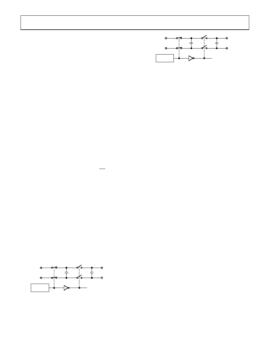
Charge Pump DC-to-DC Voltage Converter
The charge pump voltage converter consists of an oscillator and
a switching matrix. The converter generates a ±10 V supply
from the 5 V input. This is done in two stages using a switched
capacitor technique, as illustrated in Figure 22 and Figure 23.
First, the 5 V input supply is doubled to 10 V using capacitor
C1 as the charge storage element. The 10 V level is then
inverted to generate –10 V using C2 as the storage element.
+
VCC
GND
S1
S2
C1
S3
S4
C3
VCC
V+ = 2VCC
INTERNAL
OSCILLATOR
00067-0-022
Figure 22. Charge Pump Voltage Doubler
+
V+
GND
S1
S2
C2
S3
S4
C4
GND
V– = –(V+)
INTERNAL
OSCILLATOR
FROM
VOLTAGE
DOUBLER
00067-0-023
Figure 23. Charge Pump Voltage Inverter
Capacitors C3 and C4 are used to reduce the output ripple.
Their values are not critical and can be reduced if higher levels
of ripple are acceptable. The charge pump capacitors C1 and C2
may also be reduced at the expense of higher output impedance
on the V+ and V– supplies.
The V+ and V– supplies may also be used to power external
circuitry if the current requirements are small.
Transmitters (Drivers)
The drivers convert TTL/CMOS input levels into EIA-232-E
output levels. With VCC = +5 V and driving a typical EIA-232-E
load, the output voltage swing is ±9 V. Even under worst-case
conditions, the drivers are guaranteed to meet the ±5 V EIA-
232-E minimum requirement.
The input threshold levels are both TTL- and CMOS-compatible
with the switching threshold set at VCC/4. With a nominal VCC =
5 V, the switching threshold is 1.25 V typical. Unused inputs
may be left unconnected, because an internal 400 k pull-up
resistor pulls them high, forcing the outputs into a low state.
As required by the EIA-232-E standard, the slew rate is limited
to less than 30 V/s, without the need for an external slew
limiting capacitor, and the output impedance in the power-off
state is greater than 300 .
Receivers
The receivers are inverting level shifters that accept EIA-232-E
input levels (±5 V to ±15 V) and translate them into 5 V TTL/
CMOS levels. The inputs have internal 5 k pull-down resistors
to ground and are also protected against overvoltages of up to
±30 V. The guaranteed switching thresholds are 0.8 V minimum
and 2.4 V maximum, well within the ±3 V EIA-232-E require-
ment. The low level threshold is deliberately positive, since it
ensures that an unconnected input will be interpreted as a
low level.
The receivers have Schmitt-trigger inputs with a hysteresis level
of 0.65 V. This ensures error-free reception for both noisy
inputs and inputs with slow transition times.
Shutdown (SD)
The ADM206–ADM211/ADM213 feature a control input that
may be used to disable the part and reduce the power consump-
ion to less than 5 W. This is very useful in battery-operated
systems. During shutdown, the charge pump is turned off, the
transmitters are disabled, and all receivers except R4 and R5 on
the ADM213 are put into a high impedance disabled state.
相关PDF资料 |
PDF描述 |
|---|---|
| AD7731BNZ | IC ADC 24BIT SIGMA-DELTA 24DIP |
| VE-26V-CU-F4 | CONVERTER MOD DC/DC 5.8V 200W |
| PX0413/10P/PC | CONN RCPT 10POS W/PINS PCB MOUNT |
| MS3102E16S-1SW | CONN RCPT 7POS BOX MNT W/SCKT |
| ADM211EARUZ-REEL7 | IC TXRX RS-232 5V 0.1UF 28TSSOP |
相关代理商/技术参数 |
参数描述 |
|---|---|
| ADM211E | 制造商:AD 制造商全称:Analog Devices 功能描述:EMI/EMC Compliant, +-15 kV ESD Protected, RS-232 Line Drivers/Receivers |
| ADM211EAR | 功能描述:IC TX/RX RS-232 5V 0.1UF 28SOIC RoHS:否 类别:集成电路 (IC) >> 接口 - 驱动器,接收器,收发器 系列:- 标准包装:27 系列:- 类型:收发器 驱动器/接收器数:3/3 规程:RS232,RS485 电源电压:4.75 V ~ 5.25 V 安装类型:表面贴装 封装/外壳:28-SOIC(0.295",7.50mm 宽) 供应商设备封装:28-SOIC 包装:管件 |
| ADM211EAR-REEL | 功能描述:IC TXRX RS-232 5V 0.1UF 28SOIC RoHS:否 类别:集成电路 (IC) >> 接口 - 驱动器,接收器,收发器 系列:- 标准包装:121 系列:- 类型:收发器 驱动器/接收器数:1/1 规程:RS422,RS485 电源电压:3 V ~ 3.6 V 安装类型:表面贴装 封装/外壳:10-WFDFN 裸露焊盘 供应商设备封装:10-DFN(3x3) 包装:管件 |
| ADM211EARS | 功能描述:IC TX/RX RS-232 5V 0.1UF 28SSOP RoHS:否 类别:集成电路 (IC) >> 接口 - 驱动器,接收器,收发器 系列:- 标准包装:27 系列:- 类型:收发器 驱动器/接收器数:3/3 规程:RS232,RS485 电源电压:4.75 V ~ 5.25 V 安装类型:表面贴装 封装/外壳:28-SOIC(0.295",7.50mm 宽) 供应商设备封装:28-SOIC 包装:管件 |
| ADM211EARS-2REEL | 制造商:Rochester Electronics LLC 功能描述: 制造商:Analog Devices 功能描述: |
发布紧急采购,3分钟左右您将得到回复。