- 您现在的位置:买卖IC网 > PDF目录375258 > ADM2483BRW (ANALOG DEVICES INC) Half-Duplex iCoupler-R Isolated RS-485 Transceiver PDF资料下载
参数资料
| 型号: | ADM2483BRW |
| 厂商: | ANALOG DEVICES INC |
| 元件分类: | 通用总线功能 |
| 英文描述: | Half-Duplex iCoupler-R Isolated RS-485 Transceiver |
| 中文描述: | LINE TRANSCEIVER, PDSO16 |
| 封装: | MS-013AA, SOIC-16 |
| 文件页数: | 15/20页 |
| 文件大小: | 308K |
| 代理商: | ADM2483BRW |
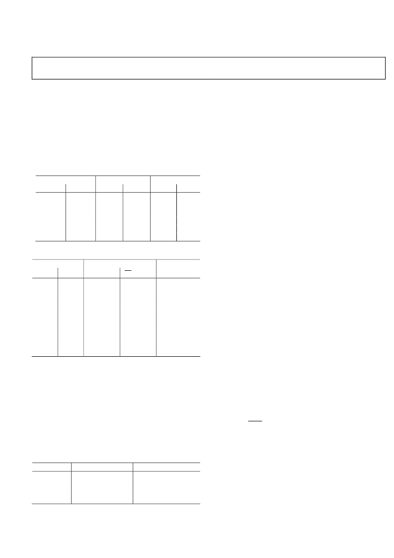
ADM2483
TRUTH TABLES
The following truth tables use these abbreviations:
Rev. 0 | Page 15 of 20
Letter
H
L
X
Z
NC
Description
High Level
Low Level
Irrelevant
High Impedance (Off)
Disconnected
Table 9.Transmitting
Supply Status
V
DD1
On
On
On
On
Off
Off
Inputs
Outputs
V
DD2
On
On
On
Off
On
Off
DE
H
H
L
X
X
X
TxD
H
L
X
X
X
X
A
H
L
Z
Z
Z
Z
B
L
H
Z
Z
Z
Z
Table 10. Receiving
Supply Status
Inputs
Outputs
V
DD1
On
On
V
DD2
On
On
A B (V)
>0.03
<0.2
0.2 < A
B < 0.03
Inputs
Open
X
X
X
X
RE
L or NC
L or NC
RxD
H
L
On
On
L or NC
Indeterminate
On
On
On
Off
Off
On
On
Off
On
Off
L or NC
H
L or NC
L or NC
L or NC
H
Z
H
H
L
POWER-UP/POWER-DOWN CHARACTERISTICS
The power-up/-down characteristics of the ADM2483 are in
accordance with the supply thresholds shown in Table 11. Upon
power-up, the ADM2483 output signals (A, B, and RxD) reach
their correct state once both supplies exceed their thresholds.
Upon power-down, the ADM2483 output signals retain their
correct state until at least one of the supplies drops below its
power-down threshold. When the V
DD1
power-down threshold
is crossed, the ADM2483 output signals reach their unpowered
states within 4 μs.
Table 11. Power-Up/Power-Down Thresholds
Supply
Transition
V
DD1
Power-Up
V
DD1
Power-Down
V
DD2
Power-Up
V
DD2
Power-Down
Threshold (V)
2.0
1.0
3.3
2.4
THERMAL SHUTDOWN
The ADM2483 contains thermal shutdown circuitry that
protects the part from excessive power dissipation during fault
conditions. Shorting the driver outputs to a low impedance
source can result in high driver currents. The thermal sensing
circuitry detects the increase in die temperature under this
condition and disables the driver outputs. This circuitry is
designed to disable the driver outputs when a die temperature
of 150°C is reached. As the device cools, the drivers are re-
enabled at a temperature of 140°C.
TRUE FAIL-SAFE RECEIVER INPUTS
The receiver inputs have a true fail-safe feature, which ensures
that the receiver output is high when the inputs are open or
shorted. During line-idle conditions, when no driver on the bus
is enabled, the voltage across a terminating resistance at the
receiver input will decay to 0 V. With traditional transceivers,
receiver input thresholds specified between 200 mV and
+200 mV mean that external bias resistors are required on A
and B pins to ensure that the receiver outputs are in a known
state. The true fail-safe receiver input feature eliminates the
need for bias resistors by specifying the receiver input threshold
between 30 mV and 200 mV. The guaranteed negative
threshold means that when the voltage between A and B decays
to 0 V, the receiver output is guaranteed to be high.
MAGNETIC FIELD IMMUNITY
The ADM2483 is immune to external magnetic fields. Its
magnetic field immunity is set when induced voltage in the
transformer’s receiving coil is large enough to either falsely set
or reset the decoder. The following analysis defines the
conditions under which this may occur. Because it represents
the most susceptible mode of operation, the ADM2483’s 3 V
operating condition is examined as an example.
The pulses at the transformer output are greater than 1.0 V in
amplitude. The decoder has sensing thresholds at about 0.5 V,
therefore establishing a 0.5 V margin in which induced voltages
can be tolerated. The voltage induced across the receiving coil is
given by
∑
=
2
n
r
dt
d
V
π
β
;
N
n
,
=
where:
β
is the magnetic flux density (Gauss).
N
is the number of turns in receiving coil.
r
n
is the radius of n
th
turn in receiving coil (cm).
Given the geometry of the receiving coil and an imposed
requirement that the induced voltage is not more than 50% of
the 0.5 V margin at the decoder, a maximum allowable
magnetic field is calculated as shown in Figure 27.
相关PDF资料 |
PDF描述 |
|---|---|
| ADM2483BRW-REEL | Half-Duplex iCoupler-R Isolated RS-485 Transceiver |
| ADM2490E | High Speed, ESD-Protected, Full-Duplex, iCoupler, Isolated RS-485 Transceiver |
| ADM2490EBRWZ | High Speed, ESD-Protected, Full-Duplex, iCoupler, Isolated RS-485 Transceiver |
| ADM2490EBRWZ-REEL71 | High Speed, ESD-Protected, Full-Duplex, iCoupler, Isolated RS-485 Transceiver |
| ADM3101E | Single Supply RS232C Line Driver/Receiver(?????μ?o?RS232C ?o?????????¨???2???2??????) |
相关代理商/技术参数 |
参数描述 |
|---|---|
| ADM2483BRW-REEL | 功能描述:IC TXRX RS-485 ISOLATED 16SOIC RoHS:否 类别:集成电路 (IC) >> 接口 - 驱动器,接收器,收发器 系列:iCoupler® 标准包装:27 系列:- 类型:收发器 驱动器/接收器数:3/3 规程:RS232,RS485 电源电压:4.75 V ~ 5.25 V 安装类型:表面贴装 封装/外壳:28-SOIC(0.295",7.50mm 宽) 供应商设备封装:28-SOIC 包装:管件 |
| ADM2483BRWZ | 功能描述:IC TXRX RS485 ISOLATED 16SOIC RoHS:是 类别:集成电路 (IC) >> 接口 - 驱动器,接收器,收发器 系列:iCoupler® 标准包装:27 系列:- 类型:收发器 驱动器/接收器数:3/3 规程:RS232,RS485 电源电压:4.75 V ~ 5.25 V 安装类型:表面贴装 封装/外壳:28-SOIC(0.295",7.50mm 宽) 供应商设备封装:28-SOIC 包装:管件 |
| ADM2483BRWZ | 制造商:Analog Devices 功能描述:RS-485 IC |
| ADM2483BRWZ-REEL | 功能描述:IC TXRX RS-485 ISOLATED 16SOIC RoHS:是 类别:集成电路 (IC) >> 接口 - 驱动器,接收器,收发器 系列:iCoupler® 标准包装:27 系列:- 类型:收发器 驱动器/接收器数:3/3 规程:RS232,RS485 电源电压:4.75 V ~ 5.25 V 安装类型:表面贴装 封装/外壳:28-SOIC(0.295",7.50mm 宽) 供应商设备封装:28-SOIC 包装:管件 |
| ADM2484E | 制造商:AD 制造商全称:Analog Devices 功能描述:500 kbps, ESD Protected, Half-/Full-Duplex, iCoupler, Isolated RS-485 Transceiver |
发布紧急采购,3分钟左右您将得到回复。