参数资料
| 型号: | ADM3252EABCZ |
| 厂商: | Analog Devices Inc |
| 文件页数: | 14/16页 |
| 文件大小: | 0K |
| 描述: | IC LINE DRIVER/RECEIVER |
| 标准包装: | 1 |
| 系列: | * |
Data Sheet
ADM3252E
Rev. A | Page 7 of 16
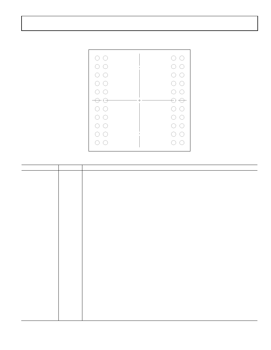
PIN CONFIGURATION AND FUNCTION DESCRIPTIONS
Figure 2. Pin Configuration
Table 6. Pin Function Descriptions
Pin No.
Mnemonic
Description
A1, L1
NC
No Connect. These pins are left unconnected.
A2, B1, B2
VCC
Power Supply Input. A 10 μF and a 0.1 μF decoupling capacitor are required between VCC and ground.
The device requires a voltage between 3.0 V and 5.5 V.
A10, B10, C10
VISO
Supply Voltage for Isolator Secondary Side. A 10 μF and a 0.1 μF decoupling capacitor are required
between VISO and ground.
A11, L11
DNC
Do Not Connect. Do not connect or route anything through these pins.
B11
V+
Internally Generated Positive Supply.
C1, C2, D2, E1, E2,
F2, G1, G2, H2, J1,
J2, K2, L2
GND
Ground Reference for Logic Side.
C11, E11, G10, G11
C1+, C1,
C2, C2+
Positive and Negative Connections for Charge Pump Capacitors. External Capacitors C1 and C2 are
connected between these pins; a 0.1 μF capacitor is recommended, but larger capacitors of up to 10 μF
can be used.
D1
TIN1
Transmitter (Driver) Input 1. A logic low on this input generates a high on TOUT1; a logic high on this
input generates a low on TOUT1. This pin accepts TTL/CMOS levels. This is a high impedance input pin;
therefore, it should not be left floating.
D10, E10, F10, H10,
J10, K10, L10
GNDISO
Ground Reference for Isolated RS-232 Side.
D11
TOUT1
Transmitter (Driver) Output 1. This pin outputs RS-232 signal levels.
F1
TIN2
Transmitter (Driver) Input 2. A logic low on this input generates a high on TOUT2; a logic high on this
input generates a low on TOUT2. This pin accepts TTL/CMOS levels. This is a high impedance input pin;
therefore, it should not be left floating.
F11
TOUT2
Transmitter (Driver) Output 2. This pin outputs RS-232 signal levels.
H1
ROUT1
Receiver Output 1. This pin outputs CMOS logic levels.
H11
RIN1
Receiver Input 1. A logic low on this input generates a high on ROUT1; a logic high on this input generates a
low on ROUT1. This input pin accepts RS-232 signal levels and has an internal 5 kΩ pull-down resistor.
J11
V
Internally Generated Negative Supply.
K1
ROUT2
Receiver Output 2. This pin outputs CMOS logic levels.
K11
RIN2
Receiver Input 2. A logic low on this input generates a high on ROUT2; a logic high on this input generates a
low on ROUT2. This input pin accepts RS-232 signal levels and has an internal 5 kΩ pull-down resistor.
105
15-
00
2
A
123
45678
9
10
11
B
C
D
E
F
G
H
J
K
L
BALLS IN COLUMN 3 TO
COLUMN 9 REMOVED
FOR ISOLATION
TOP VIEW
(Not to Scale)
ADM3252E
VCC
GND
NC
VCC
GND
TIN1
GND
TIN2
GND
ROUT1
GND
ROUT2
NC
VISO
GNDISO
C2–
GNDISO
DNC
V+
C1+
TOUT1
C1–
TOUT2
C2+
RIN1
V–
RIN2
DNC
相关PDF资料 |
PDF描述 |
|---|---|
| ADM3311EACPZ | IC TXRX RS-232 3:5 2.7V 32LFCSP |
| ADM3488EARZ | IC TXRX ESD RS-485 3.3V 8-SOIC |
| ADM3491ARU-1REEL7 | IC TXRX RS-485 HS 3.3V 16TSSOP |
| ADM3493ARZ-REEL7 | IC TXRX RS-422/485 3.3V 8-SOIC |
| ADM483EAN | IC TX/RX RS-485 LO-SLEW 5V 8DIP |
相关代理商/技术参数 |
参数描述 |
|---|---|
| ADM3260ARSZ | 功能描述:I2C Digital Isolator 2500Vrms 2 Channel 25kV/μs CMTI 20-SSOP (0.209", 5.30mm Width) 制造商:analog devices inc. 系列:IsoPower?,iCoupler? 包装:管件 零件状态:有效 技术:磁耦合 类型:I2C 隔离式电源:是 通道数:2 输入 - 输入侧 1/输入侧 2:2/2 通道类型:双向 电压 - 隔离:2500Vrms 共模瞬态抗扰度(最小值):25kV/μs 数据速率:- 传播延迟 tpLH / tpHL(最大值):- 脉宽失真(最大):145ns,85ns 上升/下降时间(典型值):- 电压 - 电源:3 V ~ 5.5 V 工作温度:-40°C ~ 105°C 封装/外壳:20-SSOP(0.209",5.30mm 宽) 供应商器件封装:20-SSOP 标准包装:66 |
| ADM3260ARSZ-RL7 | 功能描述:I2C Digital Isolator 2500Vrms 2 Channel 25kV/μs CMTI 20-SSOP (0.209", 5.30mm Width) 制造商:analog devices inc. 系列:IsoPower?,iCoupler? 包装:剪切带(CT) 零件状态:有效 技术:磁耦合 类型:I2C 隔离式电源:是 通道数:2 输入 - 输入侧 1/输入侧 2:2/2 通道类型:双向 电压 - 隔离:2500Vrms 共模瞬态抗扰度(最小值):25kV/μs 数据速率:- 传播延迟 tpLH / tpHL(最大值):- 脉宽失真(最大):145ns,85ns 上升/下降时间(典型值):- 电压 - 电源:3 V ~ 5.5 V 工作温度:-40°C ~ 105°C 封装/外壳:20-SSOP(0.209",5.30mm 宽) 供应商器件封装:20-SSOP 标准包装:1 |
| ADM32845003 | 制造商:LG Corporation 功能描述:Exchanger Assembly |
| ADM32845004 | 制造商:LG Corporation 功能描述:Exchanger Assembly |
| ADM32845010 | 制造商:LG Corporation 功能描述:Exchanger Assembly |
发布紧急采购,3分钟左右您将得到回复。