- 您现在的位置:买卖IC网 > PDF目录10181 > ADM3307EACPZ-REEL (Analog Devices Inc)IC TXRX RS-232 5:3 2.7V 32LFCSP PDF资料下载
参数资料
| 型号: | ADM3307EACPZ-REEL |
| 厂商: | Analog Devices Inc |
| 文件页数: | 5/24页 |
| 文件大小: | 0K |
| 描述: | IC TXRX RS-232 5:3 2.7V 32LFCSP |
| 标准包装: | 5,000 |
| 类型: | 收发器 |
| 驱动器/接收器数: | 5/3 |
| 规程: | RS232 |
| 电源电压: | 2.7 V ~ 3.6 V |
| 安装类型: | 表面贴装 |
| 封装/外壳: | 32-VFQFN 裸露焊盘,CSP |
| 供应商设备封装: | 32-LFCSP-VQ(5x5) |
| 包装: | 带卷 (TR) |
Data Sheet
ADM3307E/ADM3310E/ADM3311E/ADM3312E/ADM3315E
Rev. I | Page 13 of 24
CIRCUIT DESCRIPTION
The internal circuitry consists mainly of four sections. These
include the following:
A charge pump voltage converter
3.3 V logic to EIA-232 transmitters
EIA-232 to 3.3 V logic receivers
Transient protection circuit on all I/O lines
Charge Pump DC-to-DC Voltage Converter
The charge pump voltage converter consists of a 250 kHz (300 kHz
for ADM3307E) oscillator and a switching matrix. The converter
generates a ±9 V supply from the input 3.0 V level. This is done in
two stages using a switched capacitor technique. First, the 3.0 V
input supply is tripled to 9.0 V using Capacitor C4 as the charge
storage element. The +9.0 V level is then inverted to generate 9.0
V using C5 as the storage element.
However, it should be noted that, unlike other charge pump dc-
to-dc converters, the charge pump on the ADM3307E does not
run open-loop. The output voltage is regulated to ±7.25 V (or
±6.5 V for the ADM3310E and ADM3315E) by the Green Idle
circuit and never reaches ±9 V in practice. This saves power as
well as maintains a more constant output voltage.
+
GND
C2
C1
S1
S2
S3
S4
C4
VCC
S5
S6
S7
+
V+ = 3VCC
VCC
INTERNAL
OSCILLATOR
VCC
0
29
15-
0
24
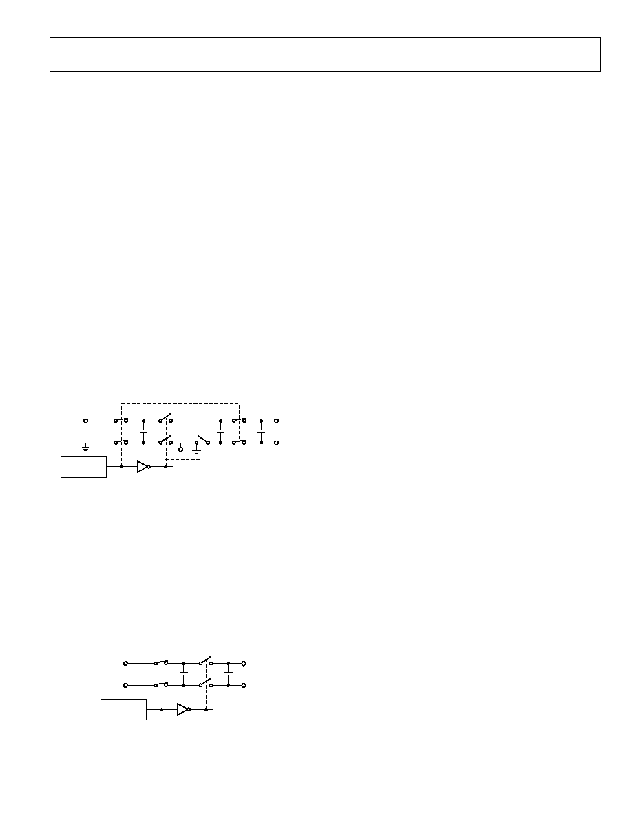
Figure 24. Charge Pump Voltage Tripler
The tripler operates in two phases. During the oscillator low
phase, S1 and S2 are closed and C1 charges rapidly to VCC. S3,
S4, and S5 are open, and S6 and S7 are closed.
During the oscillator high phase, S1 and S2 are open, and S3
and S4 are closed, so the voltage at the output of S3 is 2VCC. This
voltage is used to charge C2. In the absence of any discharge
current, C2 charges up to 2VCC after several cycles. During the
oscillator high phase, as previously mentioned, S6 and S7 are
closed, so the voltage at the output of S6 is 3VCC. This voltage is
then used to charge C3. The voltage inverter is illustrated in
+
GND
C3
S8
S9
S10
S11
C5
V– = –(V+)
+
GND
V+
INTERNAL
OSCILLATOR
FROM
VOLTAGE
TRIPLER
02
91
5-
0
25
Figure 25. Charge Pump Voltage Inverter
During the oscillator high phase, S10 and S11 are open, while
S8 and S9 are closed. C3 is charged to 3VCC from the output of
the voltage tripler over several cycles. During the oscillator low
phase, S8 and S9 are open, while S10 and S11 are closed. C3 is
connected across C5, whose positive terminal is grounded and
whose negative terminal is the V output. Over several cycles,
C5 charges to 3 VCC.
The V+ and V supplies may also be used to power external
circuitry if the current requirements are small. See Figure 12 in
What Is Green Idle?
Green Idle is a method of minimizing power consumption
under idle (no transmit) conditions while still maintaining the
ability to transmit data instantly.
How Does it Work?
Charge pump type dc-to-dc converters used in RS-232 line
drivers normally operate open-loop, that is, the output voltage
is not regulated in any way. Under light load conditions, the
output voltage is close to twice the supply voltage for a doubler
and three times the supply voltage for a tripler, with very little
ripple. As the load current increases, the output voltage falls and
the ripple voltage increases.
Even under no-load conditions, the oscillator and charge pump
operate at a very high frequency with consequent switching
losses and current drain.
Green Idle works by monitoring the output voltage and
maintaining it at a constant value of around 7 V1. When the
voltage rises above 7.25 V2 the oscillator is turned off. When the
voltage falls below 7 V1, the oscillator is turned on and a burst of
charging pulses is sent to the reservoir capacitor. When the
oscillator is turned off, the power consumption of the charge
pump is virtually zero, so the average current drain under light
load conditions is greatly reduced.
1 For ADM3310E and ADM3315E, replace with 6.5 V.
2 For ADM3310E and ADM3315E, replace with 6.25 V.
相关PDF资料 |
PDF描述 |
|---|---|
| PX0749/S | CONN RCPT 4POS W/SOCKET |
| LTC2850CMS8#TRPBF | IC TXRX RS485 20MBPS 8-MSOP |
| D7FBX | CONN RCPT FEMALE 7PIN BLK/SILVER |
| ADM3312EARUZ-REEL7 | IC TXRX RS-232 3:3 2.7V 24TSSOP |
| MS27474T18B32PA | CONN RCPT 32POS JAM NUT W/PINS |
相关代理商/技术参数 |
参数描述 |
|---|---|
| ADM3307EACPZ-REEL7 | 功能描述:IC TXRX RS-232 5:3 2.7V 32LFCSP RoHS:是 类别:集成电路 (IC) >> 接口 - 驱动器,接收器,收发器 系列:- 标准包装:121 系列:- 类型:收发器 驱动器/接收器数:1/1 规程:RS422,RS485 电源电压:3 V ~ 3.6 V 安装类型:表面贴装 封装/外壳:10-WFDFN 裸露焊盘 供应商设备封装:10-DFN(3x3) 包装:管件 |
| ADM3307EARU | 功能描述:IC TXRX RS-232 5:3 2.7V 28TSSOP RoHS:否 类别:集成电路 (IC) >> 接口 - 驱动器,接收器,收发器 系列:- 标准包装:27 系列:- 类型:收发器 驱动器/接收器数:3/3 规程:RS232,RS485 电源电压:4.75 V ~ 5.25 V 安装类型:表面贴装 封装/外壳:28-SOIC(0.295",7.50mm 宽) 供应商设备封装:28-SOIC 包装:管件 |
| ADM3307EARU-REEL | 制造商:Analog Devices 功能描述:Quint Transmitter Triple Receiver RS-232 28-Pin TSSOP T/R |
| ADM3307EARU-REEL7 | 功能描述:IC TXRX RS-232 5:3 2.7V 28TSSOP RoHS:否 类别:集成电路 (IC) >> 接口 - 驱动器,接收器,收发器 系列:- 标准包装:121 系列:- 类型:收发器 驱动器/接收器数:1/1 规程:RS422,RS485 电源电压:3 V ~ 3.6 V 安装类型:表面贴装 封装/外壳:10-WFDFN 裸露焊盘 供应商设备封装:10-DFN(3x3) 包装:管件 |
| ADM3307EARUZ | 功能描述:IC TXRX RS-232 5:3 2.7V 28TSSOP RoHS:是 类别:集成电路 (IC) >> 接口 - 驱动器,接收器,收发器 系列:- 产品培训模块:RS-232 & USB Transceiver 标准包装:2,000 系列:- 类型:收发器 驱动器/接收器数:1/1 规程:RS232 电源电压:3 V ~ 5.5 V 安装类型:表面贴装 封装/外壳:16-SSOP(0.209",5.30mm 宽) 供应商设备封装:16-SSOP 包装:带卷 (TR) 其它名称:296-19849-2 |
发布紧急采购,3分钟左右您将得到回复。