- 您现在的位置:买卖IC网 > PDF目录10798 > ADM560JRZ (Analog Devices Inc)IC TXRX RS232 4:5 3.3V LP 28SOIC PDF资料下载
参数资料
| 型号: | ADM560JRZ |
| 厂商: | Analog Devices Inc |
| 文件页数: | 11/12页 |
| 文件大小: | 0K |
| 描述: | IC TXRX RS232 4:5 3.3V LP 28SOIC |
| 标准包装: | 27 |
| 类型: | 收发器 |
| 驱动器/接收器数: | 4/5 |
| 规程: | RS232 |
| 电源电压: | 3 V ~ 3.6 V |
| 安装类型: | 表面贴装 |
| 封装/外壳: | 28-SOIC(0.295",7.50mm 宽) |
| 供应商设备封装: | 28-SOIC W |
| 包装: | 管件 |
ADM560/ADM561
Rev. B | Page 8 of 12
THEORY OF OPERATION
The ADM560/ADM561 are RS-232 transmission line drivers/
receivers, and operate from a single +3.3 V supply. This is achieved
by integrating step-up voltage converters and level shifting trans-
mitters and receivers onto the same chip. CMOS technology is
used to keep the power dissipation at an absolute minimum.
The ADM560/ADM561 are a modification, enhancement, and
improvement to the ADM241L family and its derivatives thereof.
These devices are essentially plug-in compatible and do not
have materially different applications.
The ADM560/ADM561 contain an internal voltage doubler
and a voltage inverter that generates ±6.6 V from the +3.3 V
input. Four external 1 μF capacitors are required for the inter-
nal voltage converters.
CIRCUIT DESCRIPTION
The internal circuitry consists of three main sections. These are
as follows:
A charge pump voltage converter.
3 V logic to EIA-232 transmitters.
EIA-232 to 3 V logic receivers.
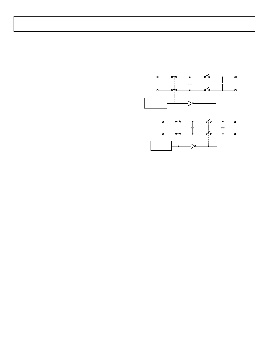
Charge Pump DC-to-DC Voltage Converter
The charge pump voltage converter consists of an oscillator and
a switching matrix. The converter generates a ±6.6 V supply from
the input +3.3 V level. This is done in two stages using a switched
+3.3 V input supply is doubled to +6.6 V using Capacitor C1
as the charge storage element. The +6.6 V level is then inverted
to generate 6.6 V using Capacitor C2 as the storage element.
Capacitor C3 and Capacitor C4 are used to reduce the output
ripple. Their values are not critical and can be reduced if higher
levels of ripple are acceptable. The C1 and C2 charge pump capac-
itors can also be reduced at the expense of the higher output
impedance on the V+ and V supplies.
The V+ and V supplies are also used to power external
circuitry if the current requirements are small.
Transmitter (Driver) Section
The drivers convert 3 V or 5 V logic input levels into EIA-232
output levels. With VCC = +3.3 V and driving an EIA-232 load,
the output voltage swing is typically ±5.5 V.
+
C3
+
C1
VCC
GND
S1
S2
S3
S4
INTERNAL
OSCILLATOR
V+ = 2VCC
VCC
056
67
-0
03
Figure 11. Charge Pump Voltage Double Operation
+
C4
+
C2
V+
GND
S1
S2
S3
S4
INTERNAL
OSCILLATOR
GND
V– = – (V+)
FROM
VOLTAGE
DOUBLER
056
67
-0
04
Figure 12. Charge Pump Voltage Inverted Operation
Unused inputs can be left unconnected as an internal 400 kΩ
pull-up resistor pulls them high forcing the outputs into a low
state. The input pull-up resistors typically source 8 μA when
grounded, so connect unused inputs to VCC or leave unconnec-
ted in order to minimize power consumption.
Receiver Section
The receivers are inverting level shifters; they accept EIA-232
input levels and translate them into 3 V logic output levels. The
inputs have internal 5 kΩ pull-down resistors to ground and are
also protected against overvoltages of up to ±25 V. The guaranteed
switching thresholds are 0.4 V minimum and 2.4 V maximum.
Unconnected inputs are pulled to 0 V by the internal 5 kΩ pull-
down resistor. This results in a Logic 1 output level for unconnected
inputs or for inputs connected to GND.
The receivers have a Schmitt trigger input with a hysteresis level
of 0.3 V. This ensures error-free reception for both noisy inputs
and for inputs with slow transition times.
ENABLE AND SHUTDOWN
Table 4 shows the truth table for the enable and shutdown
control signals. When disabled all receivers are placed in a
high impedance state. In shutdown, all transmitters are disa-
bled and all receivers on the ADM561 are disabled. On the
ADM560, Receiver R4 and Receiver R5 remain enabled in
shutdown.
相关PDF资料 |
PDF描述 |
|---|---|
| VE-JNM-MW-F1 | CONVERTER MOD DC/DC 10V 100W |
| LTC2863IDD-1#PBF | IC TRANSCEIVER RS485 8-DFN |
| VI-J5Z-MW-S | CONVERTER MOD DC/DC 2V 40W |
| KSZ9021RN | IC TXRX 10/100/1000 SGL 48QFN |
| VI-J5Y-MY-S | CONVERTER MOD DC/DC 3.3V 33W |
相关代理商/技术参数 |
参数描述 |
|---|---|
| ADM560JRZ-REEL | 功能描述:IC TXRX RS232 4:5 3.3V LP 28SOIC RoHS:是 类别:集成电路 (IC) >> 接口 - 驱动器,接收器,收发器 系列:- 标准包装:27 系列:- 类型:收发器 驱动器/接收器数:3/3 规程:RS232,RS485 电源电压:4.75 V ~ 5.25 V 安装类型:表面贴装 封装/外壳:28-SOIC(0.295",7.50mm 宽) 供应商设备封装:28-SOIC 包装:管件 |
| ADM561 | 制造商:AD 制造商全称:Analog Devices 功能描述:Ultralow Power, +3.3 V, RS-232 Notebook PC Serial Port Drivers/Receivers |
| ADM561AR | 制造商:Rochester Electronics LLC 功能描述:- Bulk |
| ADM561ARS | 制造商:Rochester Electronics LLC 功能描述:- Bulk |
| ADM561JR | 功能描述:IC TXRX RS232 4:5 3.3V LP 28SOIC RoHS:否 类别:集成电路 (IC) >> 接口 - 驱动器,接收器,收发器 系列:- 标准包装:27 系列:- 类型:收发器 驱动器/接收器数:3/3 规程:RS232,RS485 电源电压:4.75 V ~ 5.25 V 安装类型:表面贴装 封装/外壳:28-SOIC(0.295",7.50mm 宽) 供应商设备封装:28-SOIC 包装:管件 |
发布紧急采购,3分钟左右您将得到回复。