- 您现在的位置:买卖IC网 > PDF目录15341 > ADM690AARN (Analog Devices Inc)IC SUPERVISOR MPU 4.65 WD 8SOIC PDF资料下载
参数资料
| 型号: | ADM690AARN |
| 厂商: | Analog Devices Inc |
| 文件页数: | 5/8页 |
| 文件大小: | 0K |
| 描述: | IC SUPERVISOR MPU 4.65 WD 8SOIC |
| 标准包装: | 98 |
| 类型: | 备用电池电路 |
| 监视电压数目: | 1 |
| 输出: | 推挽式,图腾柱 |
| 复位: | 低有效 |
| 复位超时: | 最小为 140 ms |
| 电压 - 阀值: | 4.65V |
| 工作温度: | -40°C ~ 85°C |
| 安装类型: | 表面贴装 |
| 封装/外壳: | 8-SOIC(0.154",3.90mm 宽) |
| 供应商设备封装: | 8-SOIC |
| 包装: | 管件 |
�� �
�
�ADM690A/ADM692A/ADM802L/M/ADM805L/M�
�V� BATT�
�+5V�
�V� CC�
�BATTERY�
�SWITCHOVER�
�V� OUT�
�V� CC�
�V� OUT�
�0V�
�4.65V*�
�RESET�
�GENERATOR�
�RESET�
�(RESET)�
�0V�
�+5V�
�3.0V�
�t� RS�
�RESET�
�WATCHDOG�
�INPUT� (WDI)�
�WATCHDOG�
�TRANSITION� DETECTOR�
�(1.6s)�
�ADM690A�
�ADM692A�
�ADM802L�
�ADM802M�
�RESET�
�0V�
�+5V�
�3.0V�
�ADM805L�
�0V�
�POWER� FAIL�
�INPUT� (PFI)�
�ADM805M�
�1.25V�
�*4.4V� FOR� ADM692A/ADM802M/ADM805M�
�POWER� FAIL�
�OUTPUT� (PFO)�
�PFO�
�+5V�
�0V�
�V� BATT� =� PFI� =� 3.0V�
�(� )� =� ADM805L/M� ONLY�
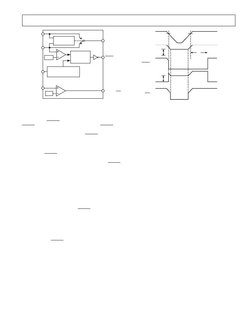
�Figure� 7.� Functional� Block� Diagram�
�POWER� FAIL� RESET� ,� RESET�
�RESET� is� an� active� low� output� which� provides� a� RESET� signal�
�to� the� microprocessor� whenever� V� CC� is� at� an� invalid� level.� When�
�V� CC� falls� below� the� reset� threshold,� the� RESET� output� is� forced�
�low.� The� nominal� reset� voltage� threshold� is� 4.65� V� (ADM690A/�
�ADM802L/ADM805L� or� 4.4� V� ADM692A/ADM802M/�
�ADM805M.�
�On� power-up� RESET� will� remain� low� for� 200� ms� after� V� CC� rises�
�above� the� reset� threshold.� This� allows� time� for� the� power� supply�
�and� microprocessor� to� stabilize.� On� power-down,� the� RESET�
�output� remains� low� with� V� CC� as� low� as� 1� V.� This� ensures� that�
�the� microprocessor� is� held� in� a� stable� shutdown� condition.�
�The� guaranteed� minimum� and� maximum� thresholds� are� as� follows:�
�ADM690A/ADM802L/ADM805L:� 4.5� V� and� 4.75� V�
�ADM692A:� 4.25� V� and� 4.5� V.�
�ADM802L:� 4.55� V� and� 4.7� V�
�ADM802M:� 4.3� V� and� 4.45� V�
�The� ADM805L� and� ADM805M� contain� an� active� high� reset�
�output.� This� is� the� complement� of� RESET� and� is� intended� for�
�processors� requiring� an� active� high� RESET� signal.�
�The� guaranteed� minimum� and� maximum� thresholds� for� the�
�ADM805� are:�
�ADM805L:� 4.5� V� and� 4.75� V�
�ADM805M:� 4.25� V� and� 4.5� V.�
�Watchdog� Timer� RESET� ,� RESET�
�The� watchdog� timer� circuit� monitors� the� activity� of� the� micro-�
�processor� in� order� to� check� that� it� is� not� stalled� in� an� indefinite�
�loop.� An� output� line� on� the� processor� is� used� to� toggle� the�
�Watchdog� Input� (WDI)� line.� If� this� line� is� not� toggled� within�
�1.6� seconds,� a� RESET� pulse� is� generated.� The� watchdog�
�timeout� period� restarts� with� each� transition� on� the� WDI� pin.� To�
�ensure� that� the� watchdog� timer� does� not� time� out,� either� a�
�high-to-low� or� low-to-high� transition� on� the� WDI� pin� must�
�occur� at� or� less� than� the� minimum� timeout� period.� If� WDI�
�remains� permanently� either� high� or� low,� reset� pulses� will� be�
�issued� after� each� timeout� period� (1.6� s).� The� watchdog� monitor�
�can� be� deactivated� by� floating� the� Watchdog� Input� (WDI)� or� by�
�connecting� it� to� midsupply.�
�REV.� 0�
�Figure� 8.� Timing� Diagram�
�BATTERY� SWITCHOVER� SECTION�
�During� normal� operation� with� V� CC� higher� than� the� reset�
�threshold,� V� CC� is� internally� switched� to� V� OUT� via� an� internal�
�PMOS� transistor� switch.� This� switch� has� a� typical� on-resistance�
�of� less� than� 1� ?� and� can� supply� up� to� 100� mA� at� the� V� OUT�
�terminal.� Once� V� CC� falls� below� the� reset� threshold,� the� higher� of�
�V� CC� or� V� BATT� is� switched� to� V� OUT� .� This� means� that� V� BATT�
�connects� to� V� OUT� only� when� V� CC� is� below� the� reset� threshold�
�and� V� BATT� is� greater� than� V� CC� .�
�V� OUT� is� normally� used� to� drive� a� RAM� memory� bank� which�
�may� require� instantaneous� currents� of� greater� than� 100� mA.� If�
�this� is� the� case,� then� a� bypass� capacitor� should� be� connected� to�
�V� OUT� .� The� capacitor� will� provide� the� peak� current� transients� to� the�
�RAM.� A� capacitance� value� of� 0.1� μ� F� or� greater� may� be� used.�
�A� 9� ?� MOSFET� switch� connects� the� V� BATT� input� to� V� OUT�
�during� battery� backup.� This� MOSFET� has� very� low� input-to-�
�output� differential� (dropout� voltage)� at� the� low� current� levels�
�required� for� battery� backup� of� CMOS� RAM� or� other� low� power�
�CMOS� circuitry.� The� supply� current� in� battery� backup� is�
�typically� 0.05� μ� A.�
�Typically� 3� V� batteries� are� used� as� the� backup� supply.� High�
�value� capacitors,� either� standard� electrolytic� or� the� farad� size�
�double� layer� capacitors,� can� also� be� used� for� short-term� memory�
�back� up.� A� small� charging� current� of� typically� 10� nA� (0.1� μ� A�
�max)� flows� out� of� the� V� BATT� terminal.� This� current� is� useful� for�
�maintaining� rechargeable� batteries� in� a� fully� charged� condition.�
�This� extends� the� life� of� the� back� up� battery� by� compensating� for�
�its� self� discharge� current.� Also� note� that� this� current� poses� no�
�problem� when� lithium� batteries� are� used� for� back� up� since� the�
�maximum� charging� current� (0.1� μ� A)� is� safe� for� even� the� smallest�
�lithium� cells.�
�If� the� battery-switchover� section� is� not� used,� V� BATT� should� be�
�connected� to� GND� and� V� OUT� should� be� connected� to� V� CC� .�
�–5� –�
�相关PDF资料 |
PDF描述 |
|---|---|
| ELJ-RE2N7DF2 | INDUCTOR 2.7NH +-.3NH FIXED SMD |
| ELJ-RE2N2DF2 | INDUCTOR 2.2NH +-.3NH FIXED SMD |
| RCC13DREI-S93 | CONN EDGECARD 26POS .100 EXTEND |
| GSC10DREI-S93 | CONN EDGECARD 20POS .100 EYELET |
| UPS2A331MHD | CAP ALUM 330UF 100V 20% RADIAL |
相关代理商/技术参数 |
参数描述 |
|---|---|
| ADM690AARN-REEL | 功能描述:IC SUPERVISOR MPU 4.65V WD 8SOIC RoHS:否 类别:集成电路 (IC) >> PMIC - 监控器 系列:- 标准包装:1 系列:- 类型:简单复位/加电复位 监视电压数目:1 输出:开路漏极或开路集电极 复位:高有效 复位超时:- 电压 - 阀值:1.8V 工作温度:-40°C ~ 125°C 安装类型:表面贴装 封装/外壳:6-TSOP(0.059",1.50mm 宽)5 引线 供应商设备封装:5-TSOP 包装:剪切带 (CT) 其它名称:NCP301HSN18T1GOSCT |
| ADM690AARNZ | 功能描述:IC SUPERVISOR MPU 4.65 WD 8SOIC RoHS:是 类别:集成电路 (IC) >> PMIC - 监控器 系列:- 其它有关文件:STM6905 View All Specifications 标准包装:1 系列:- 类型:多压监控器 监视电压数目:5 输出:开路漏极或开路集电极 复位:低有效 复位超时:最小为 140 ms 电压 - 阀值:2.188V,2.955V,可调,可调,可调 工作温度:-40°C ~ 85°C 安装类型:表面贴装 封装/外壳:8-TSSOP,8-MSOP(0.118",3.00mm 宽) 供应商设备封装:8-TSSOP 包装:Digi-Reel® 产品目录页面:1197 (CN2011-ZH PDF) 其它名称:497-8728-6 |
| ADM690AARNZ | 制造商:Analog Devices 功能描述:Controller IC |
| ADM690AARNZ-REEL | 功能描述:IC SUPERVISOR MPU 4.65V WD 8SOIC RoHS:是 类别:集成电路 (IC) >> PMIC - 监控器 系列:- 标准包装:400 系列:- 类型:备用电池电路 监视电压数目:1 输出:开路漏极,推挽式 复位:高有效/低有效 复位超时:最小为 35 ms 电压 - 阀值:4.65V 工作温度:-40°C ~ 85°C 安装类型:表面贴装 封装/外壳:16-SOIC(0.295",7.50mm 宽) 供应商设备封装:16-SOIC W 包装:带卷 (TR) 其它名称:ADM691ARZ-REEL7TR |
| ADM690ADM695 | 制造商:AD 制造商全称:Analog Devices 功能描述:Microprocessor Supervisory Circuits |
发布紧急采购,3分钟左右您将得到回复。