- 您现在的位置:买卖IC网 > PDF目录15381 > ADM805LARNZ-REEL (Analog Devices Inc)IC SUPERVISOR MPU 4.65V WD 8SOIC PDF资料下载
参数资料
| 型号: | ADM805LARNZ-REEL |
| 厂商: | Analog Devices Inc |
| 文件页数: | 6/8页 |
| 文件大小: | 0K |
| 描述: | IC SUPERVISOR MPU 4.65V WD 8SOIC |
| 标准包装: | 2,500 |
| 类型: | 备用电池电路 |
| 监视电压数目: | 1 |
| 输出: | 推挽式,图腾柱 |
| 复位: | 高有效 |
| 复位超时: | 最小为 140 ms |
| 电压 - 阀值: | 4.65V |
| 工作温度: | -40°C ~ 85°C |
| 安装类型: | 表面贴装 |
| 封装/外壳: | 8-SOIC(0.154",3.90mm 宽) |
| 供应商设备封装: | 8-SOIC |
| 包装: | 带卷 (TR) |
�� �
�
�ADM690A/ADM692A/ADM802L/M/ADM805L/M�
�Table� I.� Input� and� Output� Status� in� Battery� Backup� Mode�
�INPUT�
�POWER�
�Signal�
�V� OUT�
�Status�
�V� OUT� is� connected� to� V� BATT� via� an� internal�
�PMOS� switch.�
�R1�
�R2�
�1.25V�
�PFI�
�(PFO)�
�TO�
�μP� NMI�
�RESET�
�RESET�
�PFI�
�PFO�
�WDI�
�Logic� low.�
�Logic� high� (ADM805L,� ADM805M).� The� open�
�circuit� output� voltage� is� equal� to� V� OUT� .�
�The� power� fail� comparator� is� disabled�
�Logic� low.�
�The� watchdog� timer� is� disabled�
�5V�
�PFO�
�R3�
�Power� Fail� Comparator�
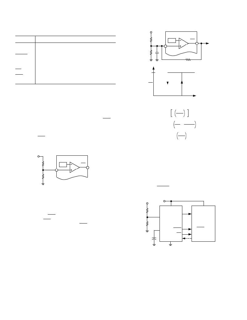
�The� power� fail� comparator� is� an� independent� comparator�
�that� may� be� used� to� monitor� the� input� power� supply.� The�
�0V�
�0V�
�V� L�
�V� H�
�comparator’s� inverting� input� is� internally� connected� to� a� 1.25�
�V� reference� voltage.� The� noninverting� input� is� available� at� the�
�V� IN�
�PFI� input.� This� input� may� be� used� to� monitor� the� input� power�
�supply� via� a� resistive� divider� network.� When� the� voltage� on� the�
�V� H� =� 1.25� 1+�
�R2+R3�
�R2� � R3�
�R1�
�PFI� input� drops� below� 1.25� V,� the� comparator� output� (� PFO� )�
�goes� low� indicating� a� power� failure.� For� early� warning� of� power�
�V� L� =� 1.25+R1�
�1.25�
�R2�
�–�
�V� CC� –1.25�
�R3�
�failure� the� comparator� may� be� used� to� monitor� the� preregulator�
�input� simply� by� choosing� an� appropriate� resistive� divider�
�network.� The� PFO� output� can� be� used� to� interrupt� the�
�processor� so� that� a� shutdown� procedure� is� implemented� before�
�V� MID� =� 1.25�
�R1+R2�
�R2�
�the� power� is� lost.�
�Figure� 10.� Adding� Hysteresis� to� the� Power� Fail�
�Comparator�
�INPUT�
�POWER�
�R1�
�R2�
�POWER�
�FAIL�
�INPUT�
�1.25V�
�(PFO)�
�POWER� FAIL�
�OUTPUT�
�TYPICAL� APPLICATIONS�
�Figure� 11� shows� a� typical� power� monitoring,� battery� backup�
�application.� V� OUT� powers� the� CMOS� RAM.� Under� normal�
�operating� conditions� with� V� CC� present,� V� OUT� is� internally�
�connected� to� V� CC� .� If� a� power� failure� occurs,� V� CC� will� decay� and�
�V� OUT� will� be� switched� to� V� BATT� thereby� maintaining� power� for�
�the� CMOS� RAM.� A� RESET� pulse� is� also� generated� when� V� CC�
�Figure� 9.� Power� Fail� Comparator�
�falls� below� the� reset� threshold.�
�Adding� Hysteresis� to� the� Power� Fail� Comparator�
�For� increased� noise� immunity,� hysteresis� may� be� added� to� the�
�UNREGULATED�
�DC�
�+5V�
�power� fail� comparator.� Since� the� comparator� circuit� is� non-�
�V� CC�
�μP� POWER�
�inverting,� hysteresis� can� be� added� simply� by� connecting� a�
�resistor� between� the� PFO� output� and� the� PFI� input� as� shown� in�
�Figure� 10.� When� PFO� is� low,� resistor� R3� sinks� current� from� the�
�summing� junction� at� the� PFI� pin.� When� PFO� is� high,� resistor�
�R3� sources� current� into� the� PFI� summing� junction.� This� results�
�R1�
�R2�
�PFI�
�V� BATT�
�V� OUT�
�RESET�
�CMOS� RAM�
�POWER�
�μP� SYSTEM�
�μP� RESET�
�in� differing� trip� levels� for� the� comparator.� Further� noise�
�immunity� may� be� achieved� by� connecting� a� capacitor� between�
�BATTERY�
�+�
�GND�
�PFO�
�WDI�
�μP� NMI�
�I/O� LINE�
�PFI� and� GND.�
�Figure� 11.� Typical� Application� Circuit�
�The� watchdog� timer� input� (WDI)� monitors� an� I/O� line� from� the�
�μ� P� system.� This� line� must� be� toggled� once� every� 1.6� seconds� to�
�verify� correct� software� execution.� Failure� to� toggle� the� line�
�indicates� that� the� μ� P� system� is� not� correctly� executing� its�
�program� and� may� be� tied� up� in� an� endless� loop.� If� this� happens,�
�a� reset� pulse� is� generated� to� initialize� the� processor.�
�–6� –�
�REV.� 0�
�相关PDF资料 |
PDF描述 |
|---|---|
| H2BBT-10103-W8-ND | JUMPER-H1500TR/A3048W/H1500TR 3" |
| UPB2D101MHD1TN | CAP ALUM 100UF 200V 20% RADIAL |
| H2BBT-10103-V8-ND | JUMPER-H1500TR/A3048V/H1500TR 3" |
| GBC61DCMD-S288 | CONN EDGECARD 122POS .100 EXTEND |
| EBC61DCMI-S288 | CONN EDGECARD 122POS .100 EXTEND |
相关代理商/技术参数 |
参数描述 |
|---|---|
| ADM805LM | 制造商:AD 制造商全称:Analog Devices 功能描述:Microprocessor Supervisory Circuits |
| ADM805M | 制造商:AD 制造商全称:Analog Devices 功能描述:Microprocessor Supervisory Circuits |
| ADM805MAN | 制造商:Analog Devices 功能描述:Processor Supervisor 4.4V 4.4V 8-Pin PDIP 制造商:Analog Devices 功能描述:PROCESSOR SUPERVISOR 4.4V 100UA 8PDIP - Rail/Tube |
| ADM805MARN | 制造商:AD 制造商全称:Analog Devices 功能描述:Microprocessor Supervisory Circuits |
| ADM809 | 制造商:AD 制造商全称:Analog Devices 功能描述:Microprocessor Supervisory Circuit in 3-Pin SOT-23 |
发布紧急采购,3分钟左右您将得到回复。